
Abstract
In the present work, silicon nanowires were prepared by a thermal evaporation method. The evaporating source was a mixture of silicon and carbon nanopowders. Surface morphology, structural characteristics and emission properties of the silicon nanowires were investigated by several techniques. The results showed that the obtained products have the shape of nanowires with diameters ranging from 30 to 120 nm and lengths from 300 to 400 nm. The x-ray diffraction (XRD) patterns confirmed the presence of crystalline silicon. Transmission electron microscope (TEM) images revealed the core-shell structure of the wires. In the photoluminescence (PL) spectra recorded at room temperature, only a broad emission band peaking at about 650 nm was observed. In addition to the red emission, two other bands centered at around 455 nm and 510 nm appeared when measured at low temperatures. The origin and emission mechanism of these bands are discussed.
Export citation and abstract BibTeX RIS

Content from this work may be used under the terms of the Creative Commons Attribution-NonCommercial-ShareAlike 3.0 licence. Any further distribution of this work must maintain attribution to the author(s) and the title of the work, journal citation and DOI.
1. Introduction
Silicon nanowires (Si NWs) have attracted much attention in recent years because they exhibit different properties in comparison to their bulk counterparts [1–4]. The Si NWs have been synthesized by using different methods, such as CVD [5], laser ablation [1] and thermal evaporation [6]. Among these methods, thermal evaporation shows many advantages, especially its low cost, ease of manufacture and relatively large yield. Various materials are used as an evaporating source to grow Si NWs, namely Si powder [7], SiO powder [6, 8], or a mixture of silicon and other powders, such as Fe powder [9], SiO 2 powder [10], sulfur powder [11] and zinc sulfide powder [12]. Also, different growth mechanisms have been proposed for the formation of silicon nanowires, including vapor–liquid–solid (VLS), oxide-assisted growth (OAG) and sulfide-assisted growth.
Although crystalline silicon is the most used material in the electronics industry, bulk silicon crystal is known to be an indirect band-gap semiconductor and, consequently, it is a poor emitter of light even at low temperatures [13]. Since the discovery of porous silicon with visible emission at room temperature [14], the light-emitting properties of Si nanostructures in general, and of nanowires in particular, have attracted considerable attention and have been investigated widely [15–24]. However, the PL properties of Si NWs measured at different temperatures have not been fully explored.
In this work, we fabricated Si NWs by a thermal evaporation method in which the source material was a mixture of silicon and carbon nanopowders. The as-synthesized Si NWs were then characterized by various means to examine the morphology, microstructure, composition and photoluminescence properties. The core-shell structures, the dependence of emission band intensity on temperature and the recombination mechanism are mentioned.
2. Experimental
In this experiment, silicon substrates were firstly cleaned via a standard procedure and subsequently coated with a gold layer of about 10 nm in thickness via a sputtering technique, which later played the role of catalyst to grow Si NWs preferentially. The as-prepared substrate was then cut into smaller chips for the next growing steps. A mixture of silicon and carbon nanopowders with a weight ratio of 4 : 1, respectively, was used as the source material. The mixture contained in an aluminum boat was placed at the center of the conventionally horizontal tube furnace. The gold-coated substrates were evenly located from the source material with a distance of 15 cm in the downstream side with respect to the flow of the carrier gas, argon. Before heating, the entire furnace was purged thoroughly with a very pure argon flow of 200 standard cubic centimeters per minute (sccm) for 30 min to remove the residual gas inside the furnace. The furnace's temperature was subsequently increased to 1200 °C with a heating rate of 10 °C per minute under steady argon flow of 50 sccm. The system was kept at 1200 °C for 1 h while the argon flow rate was maintained at 100 sccm. Eventually, the furnace was cooled down to room temperature naturally.
The as-received Si NWs' characteristics were investigated using several techniques. The microstructure of the wires was examined using a field emission scanning electron microscope (FESEM 4800 Hitachi) and a TEM (JEM 1010, JEOL, Japan) with an accelerating voltage of 80 kV. The crystalline phase and composition of the samples were characterized by the XRD technique (SIEMENS D5000). Photoluminescence spectra were recorded with a luminescence spectrometer using a He–Cd laser at a wavelength of 325 nm as the excitation source.
3. Results and discussion
Figure 1 shows SEM images of as-grown Si NWs at different resolutions. It is clearly seen that prepared nanostructures on the substrate have the morphology of one-dimensional architectures. The nanowires possess an average diameter ranging from 30 to 120 nm and their lengths vary from 300 to 400 nm. On the top of each wire, a catalyst particle (Au) can be seen, indicating the VLS growth mechanism of the Si NWs.
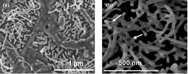
Figure 1 FESEM images of as-received Si NWs at (a) low resolution and (b) high resolution.
In order to investigate the microstructures and composition of the wires in more detail, a TEM image and an XRD pattern of the wires are obtained, as shown in figures 2 and 3. Figure 2 is the TEM image of a particular wire that has an apparent core-shell structure of amorphous SiO x – crystalline Si, respectively. The amorphous SiO x sheath envelopes entirely the inner silicon core, which is tentatively assumed to be the result of a radial oxidation process. The catalytic gold particle on the top of the wire again corroborates the validity of the VLS growth mechanism. The XRD pattern of the as-received Si NWs, shown in figure 3, reveals the dominance of the diamond structure of crystalline silicon in the sample. Besides the strong peak assigned to the Si phase, a relatively weak peak corresponding to the Au phase confirms the presence of gold particles.
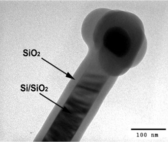
Figure 2 TEM image of a silicon nanowire. The core-shell structures as well as the presence of amorphous SiO x , crystalline Si phase and catalytic Au particles are clearly visible.
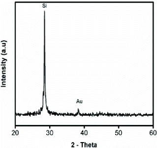
Figure 3 XRD pattern of as-grown Si NWs. Characteristic peaks attributed to diamond Si and Au phases are marked.
The PL spectra of the wires recorded at room temperature (300 K) and 10 K are presented in figures 4(a) and (b), respectively. At room temperature, a broad emission band centered on 650 nm solely predominates. Similar results are reported by several authors [13, 25–27]. It is generally accepted that the origin of this red emission band in silicon nanostructures is attributed to the quantum confinement effect. However, as mentioned earlier, the average diameter of as-grown Si NWs ranges from 30 to 80 nm, which is much larger than the Bohr radius characterized for silicon (5 nm). Fortunately, when observing carefully the TEM image of the wires in figure 2, we certainly discover the alternative presence of dark and bright layers, which denotes the SiO x and Si phases, respectively. Consequently, we propose that the core itself is an assembly of SiO x and Si regions where the dimensions of the Si regions are in the scale of its Bohr radius (5 nm). Furthermore, as examined at low temperature, 10 K, we observe two more emission bands peaking roughly at 455 nm and 510 nm in addition to the red emission band now shifted to ∼690 nm. In the literature, the blue emission band centered at around 455 nm and the 525 nm green band are attributed to the defects surrounding the silicon nanowire's crystalline core [15]. Very recently, a short-lived visible band in the photoluminescence spectrum of silicon nanocrystals that increases in intensity and shifts to longer wavelengths for smaller nanocrystals sizes was observed and assigned to the radiative recombination of non-equilibrium electron–hole pairs in a process that does not involve phonons [28].
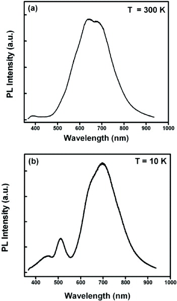
Figure 4 PL spectra of as-synthesized Si NWs measured at (a) 300 K and (b) 10 K.
The dependence of PL intensities of green and blue bands on temperature is shown in figure 5. We understandably see that the PL intensities of these two bands decrease when the temperature increases from 10 to 100 K. The result is in good agreement with that reported by Qi et al [15] in which thermal quenching is supposed to stem from the thermal ionization of charged carriers in defect centers either in the SiO x /Si interface or in the SiO x sheath [15].
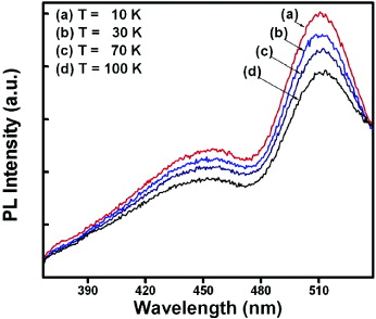
Figure 5 PL spectra of the Si NWs measured at different temperatures from 10 to 100 K and focused in the wavelength range of 360–540 nm.
Finally, we investigated the effect of the temperature on the intensities of the red emission band. The data are sketched in figure 6. It is apparently seen that the emission intensity and temperature relationship is sufficiently abnormal since the intensity firstly increases as the temperature rises from 10 to 200 K and then decreases when the temperature continues increasing from 200 K up to 300 K. This dependence does not obey the regular rule for direct-bandgap semiconductors, for which the emission band (peak) intensity reaches the maximum value at the lowest temperature. The nature of the anomalous dependence is demonstrated by Anguita et al [27] and by Brongersma et al [29], and calculated in detail by Duong et al in the case of silicon nanocrystals embedded in fused silica [30]. In these studies, the relationship is all ascribed to the singlet–triplet splitting nature of the exciton state in Si nanocrystals.
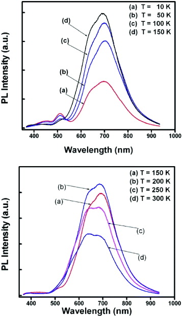
Figure 6 PL spectra of Si NWs measured at different low temperatures (left) from 10 to 150 K and (right) from 150 to 300 K.
4. Conclusion
We have successfully fabricated one-dimensional silicon nanowires via a thermal evaporation method. The as-received Si NWs exhibit an average diameter ranging from 30 to 120 nm and the lengths in the scope from 300 to 400 nm. The Si core–SiO x shell structure in which the core region consists of alternative layers of crystalline silicon and amorphous SiO x is readily observed. Several arguments are withdrawn from PL spectra of Si NWs recorded at different temperatures. At room temperature, only the intense emission band centered at 650 nm appears, whereas at low temperature (10 K) we see three emission bands peaking at roughly 455, 510 and 690 nm. The origin of the red band is supposed to be the quantum confinement effect. This effect probably results from the thin layers of crystalline silicon in the core regions. Moreover, when the temperature increases, the blue and green band intensities decrease rapidly as a result of thermal ionization of charged carriers trapped in defect centers located in the interface or shell region. On the other hand, the dependence of red emission intensity on temperature shows abnormal behavior, which is also discussed. More effort is needed to investigate further the role of the multilayer structure of Si/SiO x in the core in PL spectra as well as a quantitative explanation for the abnormal dependence.
Acknowledgments
This work was financially supported by a research project (Grant B2010-01-388) funded by the Vietnamese Ministry of Education and Training and the National Foundation for Science and Technology Development (NAFOSTED), Vietnam, under project No. 103.02.83.09 (P H D).