


Abstract
We investigate the electronic structure and the thermoelectric transport properties of zigzag buckling silicene nanoribbons (BSiNRs) under the effect of external electric fields by means of atomistic simulations. The obtained results show that thanks to the buckling feature, zigzag BSiNRs have a stronger response to a vertical electric field compared to its flat form structure and also single-layer and bi-layer graphene nanoribbons with zigzag edges (GNRs & BGNRs). An inverse is observed in the case of a transverse electric field. Interestingly, the mutual effect when applying simultaneously the vertical and transverse fields induces a larger bandgap compared to individual ones. The mutual effect observed with zigzag BSiNRs is much more pronounced compared to that in zigzag BGNRs since the vertical field has a modest effect on zigzag BGNRs stemming from weak van der Waals interactions between graphene layers. Thermoelectric performance of zigzag BSiNRs is enhanced remarkably with electric fields in which the figure of merit ZT can be tuned to exceed 1. Interestingly, although the mutual impact of two external fields induces the largest Seebeck coefficient, it unveils that the vertical electric field is overall more efficient in enhancing the thermoelectric performance of zigzag BSiNRs. In addition, the enhancement of ZT is demonstrated to stem mainly from a dramatical degradation of the electron thermal conductance around the Fermi level. This study shows that zigzag BSiNRs in combination with external electric fields have favourable advantages for different electronic and thermoelectric applications.
Export citation and abstract BibTeX RIS
1. Introduction
Over the last two decades, materials science has had huge advances since the experimental discovery of graphene, a two-dimensional material made of carbon atoms that promise a new generation of electronics [1]. This advanced material is well known for its many outstanding physical properties [2–4], in particular, its great electrical and thermal conductivity [5–7] which is potential for electronic and thermal management applications. Nonetheless, monolayer graphene exhibits semi-metallic behaviour with an almost zero-bandgap [8, 9]. It also has poor compatibility with silicon substrate [10]. These limitations result in many difficulties to take this material into practice. Therefore, scientists have been continually seeking distinct 2D materials that have physical properties similar to those of graphene but with an intrinsic bandgap or tunable electronic characteristics that could be useful for various applications and feasible in practice.
Thanks to ns2 np2 configuration with four electrons in the outer shell (in the ground state) like carbon atoms in graphene, silicon (Si) atom in group-IV elements becomes a potential candidate to constitute a 2D structure that is similar to graphene. In 2007, silicene, a 2D layer honeycomb lattice of the sp2-hybridised Si atoms was discovered [11, 12]. Based on previous studies [13, 14], the sp3-hybridisation in Si atoms has higher stability than sp2-one. Hence, scientists have studied different structures by combining sp2- and sp3- hybridised atoms to construct distinct forms of silicene that can be classified into the flat (or planar) and buckling silicene. With the structure containing sp2-hybridised Si atoms, it forms flat silicene and has a geometrical shape that is similar to graphene from the top and side views [15, 16]. In contrast, buckling silicene has a certain buckling, which forms two different planes of Si atoms. Consequently, the variation of the structure causes a diversity of the electronic properties as well as other physical ones that have attracted different research groups studying this new material [17–19].
Furthermore, the theoretical studies have indicated that the electronic structure of silicene is similar to the one of graphene with a lack of an intrinsic gap [18, 20, 21]. However, unlike graphene, silicene can grow easily on many different substrates and this is a strong advantage to make silicene compatible with current silicon technology [10, 12]. To make silicene-based electronic devices such as transistors more efficient in the operation, the first necessary is to overcome the challenge in controlling the current in such devices. Several approaches therefore have been carried out to open and modulate the energy gap of this material, such as introducing doping [22–24], defects [25], or external fields [26, 27]. Therein, by using a vertical electric field, the theoretical and experimental studies have shown that the bandgap of this material can be controlled effectively [28–30]. Ni et al [29] demonstrated that the bandgap of silicene is enlarged almost linearly with increasing strength of an applied vertical electric field. The operation of field-effect transistors based on silicene at room temperature was also discussed by Tao et al [31].
For silicene ribbons, several works have also exploited a vertical electric field to modulate the electronic properties [27, 30, 32, 33]. On the other hand, with the ribbon form, one can have the additional possibility to employ a transverse electric field to tune the electronic properties. The effect of a transverse field on the electronic properties of armchair silicene nanoribbons has been discussed by Song et al [26], and DavoodianIdalik et al [32]. Such an effect has also been investigated in zigzag silicene nanoribbons [27]. However, a comparison for the impacts of these individual fields as well as an understanding of the mutual effect of the two fields on different properties of silicene ribbons has not yet been discussed decently. In addition, the impact of these electric fields on the thermoelectric performance of silicene ribbons is also not yet paid attention.
In this study, we study systematically the individual as well as the simultaneous effects of a vertical and a transverse electric field on the electronic properties of zigzag silicene ribbons by means of atomistic simulations. Both the electronic structure and quantum transport properties are discussed. Besides, the impact of electric fields on the thermoelectric performance of zigzag silicene ribbons is also investigated. Our expectation is to provide a more comprehensive understanding of the electronic and thermoelectric properties of zigzag silicene nanoribbons in the presence of external stimuli (namely the perpendicular and transverse electric fields).
The rest of the paper is organised as follows: in section 2, we present the modelling and methodologies. Section 3 is devoted to results and discussions. In section 3.1, the electronic band structure without electric fields is investigated. In sections 3.2 and 3.3, the individual and mutual impacts of a vertical and a transverse electric field on the energy bands are discussed, respectively. In section 3.4, the thermoelectric performance of the studied system with and without electric fields is considered. Finally, conclusions are given in section 4.
2. Modelling and methodologies
2.1. Modelling
In this paper, we examine the zigzag edge of buckling silicene nanoribbons (BSiNRs) with the width W, which can also be characterised by M zigzag lines in which  where
where  is the distance between the two nearest Si-Si atoms, as shown in figure 1(a). BSiNRs contain the sp2-hybridised Si-atoms (yellow spheres) in the lower layer and the sp3-hybridised Si atoms (blue spheres) in the upper layer. The distance between these two layers is
  (as indicated in figure 1(b)). The hopping energy between the two nearest neighbouring atoms is presented by the parameter t.
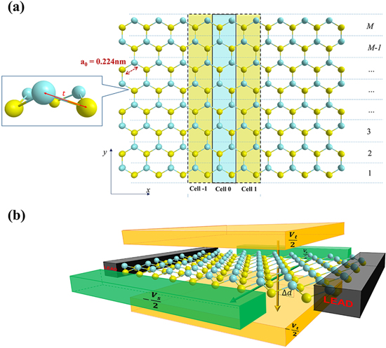
Figure 1. Illustration of (a) atomic structure of zigzag silicene nanoribbons; (b) design of electric gates to generate a vertical and a transverse electric field.
Download figure:
Standard image High-resolution imageTo investigate the effect of external electric fields, electric gates are arranged as schematised in figure 1(b). We assumed that the vertical electric field was induced by two gates as  and
and  (as indicated by orange colour), which are set up above and below the studied system, respectively. Besides, two side gates with the voltages as
  and
and  (as shown in blue colour) are designed to generate a transverse electric field along the y-axis.
2.2. Methodologies
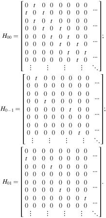
To examine the electronic properties of zigzag BSiNRs, we used the tight-binding (TB) method. The TB Hamiltonian is presented as follows [34]:

in which,  is the onsite energy of Si atom at the i-th site,
  is the energy coupling between two Si atoms at the i-th and j-th sites. It is worth mentioning that the spin-orbit coupling was not taken into account in the model (1) for the sake of simplicity and avoiding a computational burden. This model has also been considered to be appropriate for the low-energy states [34] which are the most relevant for the transport of electrons.
In our calculations, only the nearest neighbouring hopping t is considered as in [34]. The value  was taken from [19, 35]. For the flat ribbon structure of silicene,
  However, for a buckling system, an energy factor HB
(named as the buckling energy) was added to the Hamiltonian (1). Furthermore, to take into account the presence of external electric fields in calculations, beyond the components of the Hamiltonian denoted above, a matrix Uext
presenting the electrostatic potential energy induced by the external electric fields is also added and the full Hamiltonian can be rewritten as:
However, for a buckling system, an energy factor HB
(named as the buckling energy) was added to the Hamiltonian (1). Furthermore, to take into account the presence of external electric fields in calculations, beyond the components of the Hamiltonian denoted above, a matrix Uext
presenting the electrostatic potential energy induced by the external electric fields is also added and the full Hamiltonian can be rewritten as:

To be convenient in the deployment of components in equation (2), the studied zigzag BSiNRs were divided into unit cells (as illustrated in figure 1(a)) in which each unit cell contains 2 M atoms. The matrices of the Hamiltonian of a certain cell 0 and the couplings with its neighbouring cells −1 and 1 were calculated by
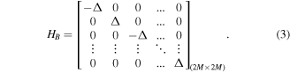
The buckling matrix HB was constructed by the parameter Δ, with Δ = 3.9 meV [35] presenting the difference of the hybridisation of Si atoms. This matrix only has nonzero terms in the main diagonal line:
The Uext
was divided into two parts for the individual contribution of the vertical and transverse electric fields:  Similar to the impact of the buckling parameter, the perpendicular electric field induces an opposite impact on atoms in the top and bottom layers (as seen in figure 1(b)) with the potentials equal to
  and
and  respectively. On the other hand, the electrostatic potential induced by the transverse electric field depends on the position of atoms, from one edge to the other one of the considered Z-BSiNR, i.e.,
  with
with  and here
 is the distance of the i-th atom along the ribbon width that is presented in table 1. The matrix form of
  is written as
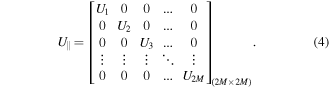
Table 1. Distance of atoms along the y-direction 

| 1 | 2 | 3 | 4 | 5 | 6 | ... | 2M-1 | 2 M |
|---|---|---|---|---|---|---|---|---|---|

|

|

|

|

|

|

| ... |

|

|
The energy bands were obtained from equation:

with 
In this work, quantum transport and the thermoelectric properties of zigzag BSiNRs were also investigated. The thermoelectric conversion is evaluated by the figure of merit  which is defined by [36]:

where  is the power factor,
  is the total thermal conductance, T is the absolute temperature. And
  and
and  are electrical conductance, Seebeck coefficient, electron thermal conductance and phonon thermal conductance, respectively. The electronic part including
  was calculated using non-equilibrium Green's function technique and the Landauer formalism, which is presented in detail in [37, 38]. The phonon conductance
  was referred from a previous study using molecular dynamics simulations [39]. It is also worth mentioning that other methodologies such as the Boltzmann transport equation can describe transport properties of both electrons and phonons. However, such a method actually considers the dynamics of particles classically [40] and lacks the capacity to treat quantum effects. On the other hand, the NEGF directly takes into account the presence of defects incorporated into the Hamiltonian and the Landauer formalism can treat the natural quantum effects of transport at the nanoscale. We therefore chose the NEGF and the Landauer formalism as relevant methods to study transport properties in this work.
3. Results and discussions
In this section, the electronic structure of zigzag BSiNRs in the absence and the presence of external electric fields is examined, respectively. Then transport properties including thermoelectrics are discussed.
3.1. Energy bands of zigzag buckling silicene nanoribbons
First, we investigate the energy bands of zigzag BSiNRs in the presence of electric fields. To better understand the difference between the electronic structure of a zigzag BSiNR and that of its counterparts, we also examine the energy bands of zigzag flat silicene nanoribbons (FSiNRs) and zigzag graphene nanoribbons (GNRs) for comparison.
In figures 2(a)–(c), the band structures of zigzag nanoribbons of width M = 12 are shown for graphene, flat silicene, and buckling silicene, respectively. As can be observed, flat bands at the zero energy are present in all the considered structures. Such flat bands are well known as edge states that are strongly localised at the two edges of the zigzag ribbon [41–43]. An energy gap is not observed in these band structures, pointing out that the metallic feature is not unique for zigzag GNRs [43, 44], but it could be a general characteristic for all ribbons with zigzag edges.
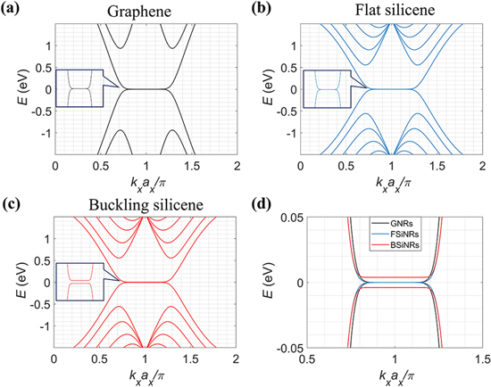
Figure 2. The band structure of different single-layer hexagonal zigzag nanoribbons (M = 12): (a) a graphene nanoribbon (GNR); (b) a flat silicene nanoribbon (FSiNR); (c) a buckling silicene nanoribbon (BSiNR); (d) comparing the energy bands around the Fermi level between these structures.
Download figure:
Standard image High-resolution imageInterestingly, comparing the dispersive parts of the lowest conduction (or the highest valence) band of these electronic structures, it is visible that the band of the zigzag GNR has a slope that is greater than the ones of the zigzag silicene ribbons (both flat and buckling forms). Such a result indicates that the electron mobility in GNRs is higher than that in other silicene structures.
To look more closely at the energy distribution around the Fermi level (E = 0), in figure 2(d) we put the energy bands of all the three structures and the narrow range of energy between −0.05 eV and 0.05 eV is examined. As can be seen, a very small gap (about 7.8 meV ≈  ) between two energy levels of the conduction and valence bands is observed in the BSiNR but not in the others, showing an interesting difference between buckling and flat layer structures. Such a result could be understood based on the hybridisation of atoms in the structure, i.e., BSiNRs consist of not only sp2-hybridised atoms (like GNRs and FSiNRs) but also sp3-hybridised atoms [12, 45, 46]. The existence of sp3 hybrid orbital weakens or leads to the disappearance of several non-local pi bonds on the surface of the material and creates asymmetry in the structure, reducing the electrical conduction of the material. FSiNRs have the same type of hybridisation (sp2) as that in GNRs, therefore they share similar electronic characteristics even though they have different bonding lengths (0.224 nm in silicene and 0.142 nm in graphene). As interesting features are observed in the electronic structure of zigzag BSiNRs, and also previous studies [17, 20] pointed out that the buckling form of silicene is more stable than the flat one, hereafter we focus mainly on zigzag BSiNRs and compare them with zigzag GNRs as candidates represent the flat structure.
3.2. Impact of individual electric fields on the band structure
In this section, the individual effects of a vertical and a transverse electric field on the energy bands of zigzag BSiNRs are considered.
3.2.1. Impact of a vertical electric field
In figures 3(a)–(c), the energy bands of a zigzag BSiNR of width M = 12 under the impact of the vertical electric field for different strengths are displayed (red curves). The results for a zigzag GNR counterpart (black curves) are also shown for comparison. As can be observed, the vertical electric fields do not lead to an opening of a bandgap in the GNR, however, it separates the flat bands of the BSiNR and enlarges the gap of this structure. The enlargement of the bandgap in the BSiNR increases with increasing magnitude of Vt , i.e., with the applied voltage Vt equal to 0.1 V, 0.3 V, and 0.5 V, the obtained bandgaps are equal to 92.2 meV, 292.2 meV, and 492.2 meV, respectively.
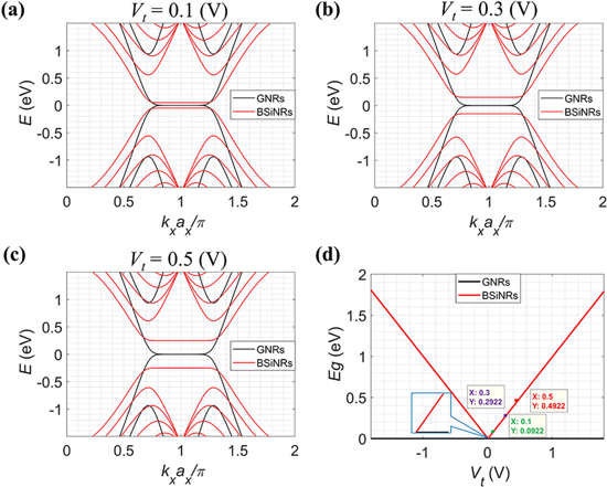
Figure 3. Energy bands under the effect of a vertical electric field: (a) Vt = 0.1 V; (b) Vt = 0.3 V; (c) Vt = 0.5 V; (d) Egap depending on the vertical potential Vt . All ribbons have the width M = 12.
Download figure:
Standard image High-resolution imageThe different phenomena in the electronic structure of the GNR and the BSiNR can be understood based on the description of the TB model presented above. In GNRs, all the carbon atoms lie on the same plane, whereas in BSiNRs, silicon atoms belong to two distinct planes due to the buckling feature of silicene in which the first plane consists of sp2- hybridised atoms, and the other plane contains hybridised ones. When a vertical electric field is applied from top to bottom (as illustrated in figure 1(b)), all carbon atoms in GNRs get the same potential from the vertical electric field, and therefore it does not lead to any difference between atoms in the system. As a result, the energy bands of GNRs are not changed in the presence of a vertical electric field. Meanwhile, for BSiNRs, atoms in the upper and lower planes obtain different potentials  and
and  respectively. This causes an increase in the energy difference between the nearest neighbouring atoms, and enlarges the bandgap in this structure. It is also worth noting that the vertical electric field opens a gap in the considered zigzag BSiNR but it does not change the form of the energy bands as seen in figures 3(a)–(c).
In figure 3(d) the bandgap in the two structures is plotted as a function of the potential of the vertical electric field. The black curve clearly indicates that the bandgap of the GNR remains to be zero regardless of the strength and the direction of the vertical field. On the other hand, the red curve reveals that the gap of the BSiNR increases linearly with increasing magnitude of the vertical electric field. By noting the fact that the intrinsic bandgap is almost equal to  that is the energy difference between the energies of the two distinct hybridised Si atoms, thus the dependence of the bandgap on the applied vertical field is expected to follow the same rule, i.e.,
  and this is in agreement with the linear behaviour seen in figure 3(d).
In conclusion, BSiNRs have been seen to be more responsive to a vertical electric field compared to GNRs thanks to the buckling feature which gains the energy difference between the different hybridised atoms. It is also worth mentioning that buckling or out-of-plane deformed graphene ribbons with zigzag edges also do not induce a bandgap under the impact of a vertical electric field due to the strong localisation of edge states at the Fermi level [47]. Thus, the obtained results for zigzag BSiNRs reveal a high potential of BSiNRs for electronic devices where the electronic performance can be flexibly controlled by an external vertical electric field.
3.2.2. Impact of a transverse electric field
To understand the role of the direction of the electric field, we continue to examine the change of the electronic structure in the presence of a transverse electric field.
Figures 4(a)–(c) show the energy bands of the BSiNRs (red line) and the GNRs (black line) for different Vs . It is clear that the transverse electric field has strong impacts on both structures and it is different from the case of the perpendicular electric field that has been considered above. The results demonstrate that the size of the gap increases remarkably in the two structures when increasing the magnitude of Vs as 0.1 V, 0.3 V, and 0.5 V, respectively.

Figure 4. (a)–(c) Energy bands of zigzag BSiNR (red line) and GNR (black line) corresponding to three different transverse electric fields: (a) Vs = 0.1 V; (b) Vs = 0.3 V; (c) Vs = 0.5 V; (d) Egap is plotted as a function of Vs . For all ribbons, M = 12.
Download figure:
Standard image High-resolution imageThe variation of the bandgap is directly associated with the change of the originally flat bands (edge states). As can be observed, unlike the case of the vertical electric field, the transverse field has a visible impact on the bands of the edge states when the field strength is significant enough as seen in figures 4(b) and (c). The effect is more pronounced at the two sides of the edge state bands near the points  and leads to an in-direct behaviour of the bandgap.
The strong impact of the transverse electric field on the edge states could be understood from the fact that this type of field induces a charge redistribution in the layer in which more electrons move closer to the positive voltage gate while holes move towards the negative ones. As a result, the highest charge density is distributed near the ribbon edges and it becomes smaller when it goes to the centre of the ribbon. Such results are consistent with previous studies [43, 44]. As edge states in zigzag structures localised at the edges, they are strongly affected by the charge redistribution caused by the external field leading to the change in the shape of the band of the edge states.
In further analysis, we considered the variation of the bandgap as a function of the applied gate voltage Vs . The results are shown in figure 4(d) for both the GNR and the BSiNR. When a weak transverse field with Vs below 0.1 V is applied, the gap in both structures is almost the same and increases linearly with increasing Vt . However, above Vt = 0.1 V, the change of the bandgap is non-linear and there is a discrepancy between the two structures in which the electric field induces a larger gap in the GNR compared to that in the BSiNR. In the range of Vt from −1.8 V to 1.8 V, the gap of the GNR reaches a maximum value of 660 meV at Vt = ±1.6 V and in the BSiNR this value is about 387.6 meV at Vt = −0.94 V.
It is worth mentioning that the variation of the bandgap in the GNR is symmetrical with respect to the sign of Vt
, however, it is slightly asymmetrical in the case of the BSiNR. Such asymmetrical effect stems from the energy difference of the two types of hybridised Si atoms in BSiNRs. Under the impact of the transverse electric field, the energies of Si atoms in the upper and lower planes of the structure are  and
and  respectively. And once the electric field reversed its direction, these energies change to
  and
and  respectively and it is clear that they are not symmetrical with the previous energies. However, because
  meV is small, the asymmetrical effect is therefore not pronounced.
3.3. Mutual effect of a vertical and a transverse electric field on the band structure
The above analyses have shown the distinct impacts of a vertical and a transverse electric field on the electronic structure of the flat (zigzag GNRs) and buckling (zigzag BSiNRs) structures. Therefore, it is worth investigating the mutual impact of these two fields on the energy bands. As the vertical electric field does not impact the electronic properties of GNRs, the mutual effect in this material is likely identical to the effect of the transverse field that is considered above. We therefore only examine the mutual effect in BSiNRs.
In figure 5 the bandgap of several zigzag BSiNRs of width M = 10, 11, 12 is plotted as a function of Vt (Vs ) for a certain magnitude of Vs (Vt ).
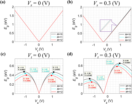
Figure 5. Egap is plotted as a function of Vt , with: (a) Vs = 0; (b) Vs = 0.3 V. Egap is plotted as a function of Vs , with: (c) Vt = 0; (d) Vt = 0.3 V.
Download figure:
Standard image High-resolution imageFirst, the results in figures 5(a)−(b) reveal that the impact of the vertical field is almost independent of the ribbon width (or the number of zigzag lines M). In the presence of a transverse field with Vs = 0.3 V (figure 5(b)), it can be seen that the gap is enlarged for all positive Vt , indicating a stronger modulation of the electronic structure when combining the two fields.
On the other hand, the variation of the gap of the considered BSiNRs without and with a transverse electric field depends on the width of the ribbon as can be clearly observed in figures 5(c) and (d). Interestingly, with the combination of the vertical field with the voltage Vt = 0.3 V, the asymmetry of the bandgap with respect to the sign of Vs becomes more remarkable as seen in figure 5(d). Besides, the maximum of the bandgaps increases from 459.3 meV, 420.5 meV, and 387.6 meV with Vt = 0 to 649.7 meV, 612.7 meV and 581.6 meV when Vt = 0.3 V for the ribbons of width M = 10, 11, 12, respectively.
To give an overview on the modulation of the electronic structure under the impacts of the two coexisting fields, the bandgap is plotted as a function of both Vt and Vs and shown in figure 6(a) for M = 12. Similar results were observed for other ribbons of width.
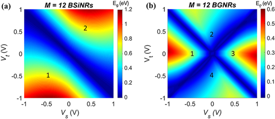
Figure 6. Bandgap is plotted as a function of Vt and Vs for (a) a zigzag BSiNR; (b) a zigzag BGNR. All structures have M = 12.
Download figure:
Standard image High-resolution imageThe result in figure 6(a) shows that the bandgap in the BSiNR is almost equal to zero if the two fields have opposite potentials Vt = −Vs . However, the gap is enlarged when the pair of the potentials [Vt , Vs ] is either in region 1 or region 2 at the two sides of the diagonal line Vt = −Vs . Interestingly, the largest gap is obtained when the two fields are applied simultaneously, i.e., Eg ≈ 1.2 eV at Vt ≈ −1 V and Vs ≈ −0.5 V
To better understand the mutual effect in the BSiNR, we make a comparison with the result obtained for a zigzag BGNR as such a structure has two layers of atoms in which both vertical and electric fields affect the electronic structure as indicated in a previous study [6]. The result for a zigzag BGNR of width M = 12 is shown in figure 6(b). As can be observed, the bandgap of the considered BGNR is classified into four regions that are defined by the cones Vs = Vt and Vs = −Vt . More importantly, although the vertical field induces an effect in the formation of the bandgap in the BGNR, its role is weak as the largest gap is obtained in the regions (1) and (3) and near the points where Vt ≈ 0. The much weaker effect of the vertical field in the BGNR compared to that in the BSiNR could be interpreted by the fact that although the vertical field induces a significant difference in the onsite energies of atoms in the upper and lower layers of the BGNR, due to the natural weakness of Van de Waals interactions between the two graphene layers, it does not lead to a strong charge redistribution between layers. In contrast, atoms in the BSiNR are also classified into two planes, but they belong to the same layer, so the interaction between atoms in the two planes is much stronger and a charge redistribution is more sensitive to an applied vertical field.
Thus, with the combination of two types of fields, the bandgap of zigzag BSiNRs could be tuned more effectively compared to that of zigzag GNRs and BGNRs. In other words, the simultaneous impact of fields on the buckling structure leads to high efficiency in the modulation of the bandgap of the material. Such results suggest that BSiNRs have favourable advantages to be exploited for different electronic applications.
3.4. Impact of external electric fields on the thermoelectric performance of zigzag BSiNRs
In this section, we consider the impact of external fields on the thermoelectric transport properties of devices made of zigzag BSiNRs. A device (as illustrated in figure 1(b)) of the length L ≈ 40 nm and the width W ≈ 3.73 nm (M = 12) was considered. The electron transmission was computed by the NEGF technique [48] and the electrical conductance  the Seebeck coefficient S, and the electron thermal conductance Ke
were calculated based on the Landauer formalism [37, 49]. The results of
the Seebeck coefficient S, and the electron thermal conductance Ke
were calculated based on the Landauer formalism [37, 49]. The results of  and the power factor
  at room temperature and under the impact of external fields are shown in figure 7.

Figure 7. (a) Electrical conductance; (b) Seebeck coefficient and (c) Power-factor without and with external fields. Inset in the panel (b) is the Seebeck coefficient in the absence of external fields. The simulations were done for M = 12 and at T = 300 K.
Download figure:
Standard image High-resolution imageAs can be observed in figure 7(a), a transport gap is opened in the electrical conductance when either a vertical or a transverse field is applied. Such gap is even wider when the two fields are employed simultaneously as can be seen from the purple (dash-dot) curve. The widening of the transport gap leads to a better separation of electrons and holes which results in a larger Seebeck coefficient as can be seen in figure 7(b). The maximum value of the intrinsic Seebeck coefficient of the ribbon in the absence of an external field is about 0.066 mW K−1 as shown in the inset in figure 7(b). This value increases to 0.33 mW K−1 and 0.69 mW K−1 when individual fields of the strengths Vs = 0.5 V and Vt = 0.5 V are applied and it even reaches 1.05 mV K−1 with the mutual effect of the two fields. It is worth mentioning that the variation of the electrical conductance and the Seebeck coefficient is fully consistent with the change in the electronic structures in the absence or the presence of external fields, i.e., the decrease (increase) of the electrical conductance (the Seebeck coefficient) around the Fermi level is proportional to the enlargement of the bandgap in the presence of an external field that has been observed in figures 3–6. Also, the quantum number of the electrical conductance (in 2e2 /h) at each energy level is equal to the number of channels that can be counted by using a line that crosses the energy bands in a single valley (+kx or −kx ) at the corresponding energy level (see figures 3, 4).
The common strategies to enhance the thermoelectric performance of a system are to increase the power factor or/and to reduce the thermal conductance [50–52]. It is therefore more relevant to consider the variation of the power factor. It can be seen in figure 7 that the maximum value of the power factor when Vt = Vs = 0 is about 0.59 pW K−2 and it increases to 0.74 pW K−2, 0.69 pW K−2 and 0.66 pW K−2 when the potentials [Vt , Vs ] are equal to [0.5 V, 0], [0, 0.5 V], and [0.5 V, 0.5 V], respectively. Thus, although the mutual effect has the most impact on the Seebeck coefficient, the vertical field is found to be overall more efficient for enhancing the power factor.
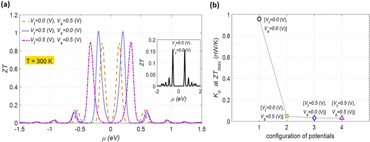
To completely evaluate the thermoelectric performance of the system that also includes the contribution of the phonon part, we calculated the figure of merit ZT by using equation (6) and the value of the phonon conductance was referred from molecular dynamic simulations that were carried out by Pan et al [39]. As the phonon conductance increases almost linearly with increasing ribbon width, we extrapolated Kp
at the width M = 12 and obtained the value of 0.1788 nW K−1. It is worth mentioning that the phonon conductance does not change when different fields are applied. Figure 8(a) display ZT for all the considered pairs of the potentials. Due to the small Seebeck coefficient,  of the ribbon in the absence of fields is only about 0.15 and this result is in agreement with that obtained in [39] by density functional theory calculations and molecular dynamic simulations. Interestingly, ZT increases remarkably with the presence of the fields, i.e.,
  equals 1.02, 0.89 and 0.90 when [Vt
, Vs
] are equal to [0.5 V, 0], [0, 0.5 V], and [0.5 V, 0.5 V], respectively. Such enhancement of ZT is about 6–7 times higher in the system without fields. To better understand the strong enhancement of ZT even though the power factor just increases not more than 1.25 times, we examined the electron thermal conductance
equals 1.02, 0.89 and 0.90 when [Vt
, Vs
] are equal to [0.5 V, 0], [0, 0.5 V], and [0.5 V, 0.5 V], respectively. Such enhancement of ZT is about 6–7 times higher in the system without fields. To better understand the strong enhancement of ZT even though the power factor just increases not more than 1.25 times, we examined the electron thermal conductance  that corresponds to the
  and the results are shown in figure 8(b). As can be observed,
  reduces about an order of magnitude when the fields are applied. The strong degradation of
  near the Fermi level is due to the widening of the bandgap that decreases the mobility of electrons. Thus, the enhancement of ZT mainly originates from the reduction of the electron thermal conductance.
Figure 8. (a) Figure of merit ZT under the impact of individual and combined fields. Inset is the result in the absence of external fields. (b) Electron thermal conductance corresponds to ZTmax for different applied fields. The simulations were done for M = 12 and at T = 300 K.
Download figure:
Standard image High-resolution image
4. Conclusion
In this paper, we have investigated the electronic structure and the thermoelectric properties of zigzag BSiNRs. It has shown that thanks to the buckling feature, zigzag BSiNRs possess unique features compared to the counterparts zigzag GNRs and also FSiNRs which exist in a planar layer. In the absence of external fields, zigzag BSiNRs exhibit semi-metallic behaviour with a small gap of about 7.8 meV due to the simultaneous existence of sp2- and sp3- hybridised atoms. The gap is almost zero in zigzag FSiNRs and zigzag GNRs. In the presence of external electric fields, it has been observed that zigzag BSiNRs are more responsive to a vertical field than a single layer and even bilayer zigzag GNRs and it is inverse with a transverse field. A vertical field can remarkably enlarge the gap of zigzag BSiNRs in which the gap increases linearly with the applied voltage, i.e.,  for all ribbons of width. The variation of the gap under the effect of a transverse electric field depends on the ribbon width and it is non-linear with increasing voltage Vs
, e.g., for M = 12 the gap reaches the maximum value of 387.6 meV at Vt
= −0.94 V. Interestingly, the gap of zigzag BSiNRs increases further under the simultaneous effect of both vertical and transverse fields, i.e., Egap
of the ribbon of width M = 12 can reach 1.2 eV at Vt
≈ −1 V and Vs
≈ −0.5 V. The mutual effect observed with zigzag BSiNRs is much more pronounced compared to that in zigzag BGNRs since the vertical field has a modest effect on zigzag BGNRs stemming from weak van der Waals interactions between graphene layers.
for all ribbons of width. The variation of the gap under the effect of a transverse electric field depends on the ribbon width and it is non-linear with increasing voltage Vs
, e.g., for M = 12 the gap reaches the maximum value of 387.6 meV at Vt
= −0.94 V. Interestingly, the gap of zigzag BSiNRs increases further under the simultaneous effect of both vertical and transverse fields, i.e., Egap
of the ribbon of width M = 12 can reach 1.2 eV at Vt
≈ −1 V and Vs
≈ −0.5 V. The mutual effect observed with zigzag BSiNRs is much more pronounced compared to that in zigzag BGNRs since the vertical field has a modest effect on zigzag BGNRs stemming from weak van der Waals interactions between graphene layers.
The thermoelectric performance of zigzag BSiNRs is also strongly modulated under the impact of external fields. The figure of merit ZT of the ribbon of width M = 12 is enhanced remarkably from 0.15 in the absence of external fields to 1.02, 0.89, and 0.90 in the presence of fields with the magnitudes of the applied voltages [Vt , Vs ] equal to [0.5 V, 0], [0, 0.5 V], and [0.5 V, 0.5 V], respectively. Although the mutual effect of two external fields induces the largest gap compared to individual fields and therefore the largest Seebeck coefficient, the results revealed that the vertical electric field is overall more efficient in enhancing the thermoelectric performance of zigzag BGNRs as this field leads to a better trade-off between the electrical conductance and the Seebeck coefficient. Interestingly, the enhancement of ZT is demonstrated to stem mainly from the decrease of the electron thermal conductance which is about an order of magnitude lower than that without external fields.
Acknowledgments
This research is funded by Vietnam National Foundation for Science and Technology Development (NAFOSTED) under grant number 103.01-2018.338.