
Abstract
This paper presents our recent theoretical and experimental study of piezo-effects in nanostructured materials for highly sensitive, high resolution mechanical sensors. The piezo-effects presented here include the piezoresistive effect in a silicon nanowire (SiNW) and single wall carbon nanotube (SWCNT) thin film, as well as the piezo-optic effect in a Si photonic crystal (PhC) nanocavity. Firstly, the electronic energy band structure of the silicon nanostructure is discussed and simulated by using the First-Principles Calculations method. The result showed a remarkably different energy band structure compared with that of bulk silicon. This difference in the electronic state will result in different physical, chemical, and therefore, sensing properties of silicon nanostructures. The piezoresistive effects of SiNW and SWCNT thin film were investigated experimentally. We found that, when the width of 〈 110 〉 p-type SiNW decreases from 500 to 35 nm, the piezoresistive effect increases by more than 60%. The longitudinal piezoresistive coefficient of SWCNT thin film was measured to be twice that of bulk p-type silicon. Finally, theoretical investigations of the piezo-optic effect in a PhC nanocavity based on Finite Difference Time Domain (FDTD) showed extremely high resolution strain sensing. These nanostructures were fabricated based on top-down nanofabrication technology. The achievements of this work are significant for highly sensitive, high resolution and miniaturized mechanical sensors.
Export citation and abstract BibTeX RIS

Content from this work may be used under the terms of the Creative Commons Attribution-NonCommercial-ShareAlike 3.0 licence. Any further distribution of this work must maintain attribution to the author(s) and the title of the work, journal citation and DOI.
1. Introduction
Recently, nanostructured materials have attracted a lot of attention in Nano ElectroMechanical Systems (NEMS) technology because of their excellent properties for highly sensitive and high resolution physical and chemical sensing applications [1–3]. Nanostructured materials, such as atomic clusters, nano dot, nano layered films, filamentary structures and bulk nanostructured materials, are referred to those materials with structural elements having nanoscale dimensions, i.e. at least one dimension in the range from 1 to 100 nm. In such low-dimensional nanostructures, due to the quantum confinement effect, the eclectic, magnetic, optical properties of materials were reported to be remarkably different from those of bulk materials, and accordingly, interesting physical and chemical sensing effects in nanostructures are also expected. For example, giant piezoresistive effects were found experimentally in SiNW [1] and SWCNT [2], an extremely high sensitive gas sensing effect in graphene nanosheet [3] and single-electron resolution electric-field sensing based on graphene nanosheets [4]. Such excellent properties are attributed to the facts that when the dimensions of materials reduce to the low-dimensional nanostructure, such as nanodot (0D), nanowire (1D) and nanosheet (2D), most atoms are exposed and the quantum confinement effect of the carriers plays a major role in determining their physical properties. Based on the first-principles calculations method, we found that low-dimensional structures such as silicon nanosheets (2D) and nanowires (1D) have very different electronic states compared to microscopic and macroscopic structures [5]. Therefore, the physical and chemical properties of such nanoscale materials should be very different from the macroscopic properties of the same substance, offering superior properties for the emerging advanced applications.
In this paper, first, the analysis of the electronic state of Si nanostructure is introduced to illustrate the different electronic state compared to that of bulk silicon. Next, fabrication and evaluation of piezoresistive effects of SiNW and SWCNT thin films are presented. Finally, a theoretical study of the piezo-optic effect in a PhC nanocavity is discussed.
2. Electronic state in silicon nanostructures
Electrical characteristics of Si materials are dominated by the electronic state. In particular, the electronic structure of the valence band (VB) of Si materials is related to the electrical properties of p-doped Si semiconductors.
Single-crystal bulk Si has an indirect band gap as is well known, where the conduction band (CB) has a multi-valley structure, and the maximum of the VB top is located at the Γ point. The three highest VB subbands are triply degenerated at the Γ point by means of non-relativistic regular first-principle calculation, though one of these subbands should be separated from the other two, the heavy-hole and light-hole bands, in the actual system because of the relativistic spin–orbit coupling. Our novel approach to simulate the piezoresistive effect has succeeded in a qualitative and quantitative estimation of the primitive piezoresistive coefficients, π11, π12 and π44, for n-type bulk Si [6], derived from the multi-valley CB structure.
The dimensional reduction to a Si(001) nanosheet brings a quasi-direct band gap, as shown in figure 1, where the minimum of the CB bottom is located at the Γï€ point due to the two-dimensional confinement of the electronic structure [7, 8]. In the VB top of the Si(001) nanosheet models, the two highest VB subbands are doubly degenerated at the Γ point by means of regular first-principle calculation, and their characteristics can correspond to the heavy-hole and light-hole bands with the spin–orbit coupling for bulk Si. However, a different electronic structure from bulk Si can be obtained as the sheet thickness is reduced. The [110] uniaxial tensile stress for the Si(001) nanosheet models causes band deformation, leading to the redistribution of carriers and a drastic change in conductivity can be observed. The p-type longitudinal and transverse piezoresistive coefficients about the [110] tensile stress [7] and shear one about (001) shear strain [8] swell up, respectively, as the nanosheet becomes thinner, and we have obtained high piezoresistive coefficients of 343×10−11 Pa −1 of π l[110], −141×10−11 Pa −1 of π t[110] and 450×10−11 Pa −1 of π s for about 1 nm thickness by a simulation on the basis of first-principle calculation.
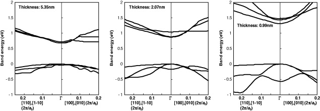
Figure 1 Band diagrams of the three lowest CB subbands and three highest VB subbands for the hydrogen-terminated Si(001) nanosheet models around the Γ point. The energy zero is defined at the valence-band top.
Through further dimensional reduction to a Si〈 001 〉 nanowire of a few nanometers radius, the electronic structure has been completely changed from that of bulk Si. The uniaxial tensile stress in the longitudinal direction causes an exchange of the order in the band energy of subbands in the VB top, and a sudden change in the hole occupation with the increase in effective mass bringing a drastic decrease in the hole conductivity. About 600×10−11 Pa −1 of π l〈001〉 is expected for p-type Si〈 001 〉 nanowire with a 2 nm diameter by our simulation [9].
3. Piezoresistive effect in silicon nanowire
The piezoresistive effect has been one of the most frequently applied principles in (MEMS) micro electro mechanical systems for developing micro mechanical sensors over the past three decades. For recently emerging applications, such as camera image stabilization, mobile phone, hard disk protection, health monitoring and so on, the sensors are required to have smaller size, higher sensitivity and lower power consumption. However, when the physical size of an inertial sensor decreases, its sensitivity is also drastically reduced by the fourth power rule. One of the solutions to overcome this problem is to realize a higher piezoresistive effect in SiNW, as briefly discussed in section 2 above and in [9].
In order to evaluate the piezoresistive effect in single crystalline SiNW, we used a cantilever model with SiNW arrays arranged on top, as shown in figure 2. Each array consists of identical SiNWs connected in parallel, and aligned with longitudinal or transverse axes of the cantilever, as shown schematically in figure 2. To investigate the piezoresistive effect in different crystallographic orientations, the SiNW arrays are aligned along different orientations, e.g. 〈 100 〉, 〈 010 〉 and 〈 110 〉 directions on the (001) single crystalline silicon SOI wafer. The width of SiNW in different arrays is different, and it ranges from 35 to 500 nm.
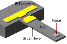
Figure 2 Cantilever model for measurement of the piezoresistive effect in SiNW.
By loading at the free end of the cantilever, the stress/strain will be generated in the SiNW and, therefore, the resistance of the SiNW is changed. Measurement of this resistance change and applied stress can provide the piezoresistive coefficients.
3.1. Fabrication of SiNWs
SiNWs are fabricated by the top-down process described in figure 3 [9]. SIMOX (Separation by Implanted Oxygen) wafer with a 50-nm-thick (100) Si device layer was used. First, boron was implanted uniformly into the 50-nm-thick Si device layer to obtain a concentration of 1.2×10¹⁸ atoms cm −3. Then, a 150-nm-thick SiO 2 layer was deposited and annealed to form a hard mask for RIE etching. Next, SiNW patterns were defined by electron beam lithography (EBL) and dilute hydrofluoric (DHF) etching of SiO 2. Then, the SiNW structures were formed by RIE of Si. A 10-nm-thick SiO 2 layer was thermally grown to deactivate the sidewall layers, which were attacked during the RIE process. Next, a 100-nm-thick SiO 2 layer was deposited to protect the SiNW. Then, contact holes were opened by HF wet etching. Finally, 50 nm- TiN/500 nm- Al were deposited, patterned and annealed to form a metal contact. Annealing was performed at a temperature of 550 °C in N 2 for 30 min.
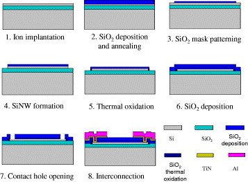
Figure 3 Schematic model for measurement of the piezoresistive effect in SiNW.
SiNW arrays with a length and thickness of 2 μm and 40 nm, respectively, and width ranges from 35–490 nm were fabricated. The resistivity of the SiNW was 0.035 Ω cm. Figure 4 shows SEM images of a fabricated SiNW array. Figure 4(a) shows a SiNW array covered by a SiO 2 layer, and figure 4(b) is a cut-away image showing SiNWs embedded completely in SiO 2. Figure 5 shows SEM images of the 〈 100 〉 and 〈 110 〉 SiNWs after the SiO 2 layer was removed to observe the actual size of the nanowires.
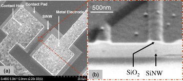
Figure 4 (a) SEM image of SiNW array and (b) FIB cutting image showing SiNWs embedded in SiO 2 layer.
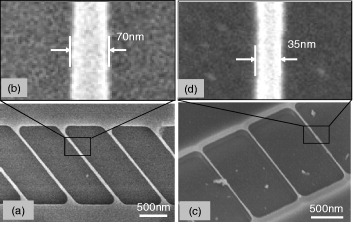
Figure 5 SiNW array without SiO 2 layer: (a) 〈 100 〉 SiNW array, (b) close-up view of (a), (c) 〈 110 〉 SiNW array (d) close-up view of (c).
3.2. Measurement of piezoresistive coefficients
Identical force is applied on the tip of the cantilever to generate stress/strain in the SiNWs, as shown in figure 2. The resistance of the SiNWs is measured by using a four-probe resistance measurement technique to eliminate the contact resistance between the SiNWs and Al interconnection wires. Figure 6 shows the resistance change in the SiNWs versus applied strain at room temperature. A linear relation between the resistance change and the applied strain was obtained. The gauge factor for the 35-nm-width SiNWs was determined to be G=91, i.e. 1.75 times larger than that of the 490-nm-width SiNWs. Figures 7 and 8 show the dependence of the longitudinal and transverse piezoresistive coefficients for the 〈 110 〉 and 〈 100 〉 directions, respectively, on the width of the SiNWs.
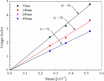
Figure 6 Resistance change in different SiNWs versus strain.
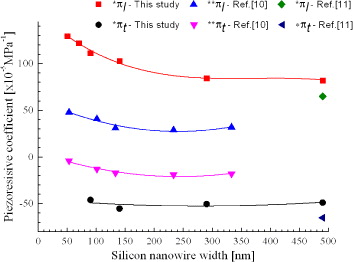
Figure 7 With dependence of piezoresistive coefficients in 〈 110 〉 crystallographic direction. Note: (*) concentration: 1.2×1018 cm −3, (**) concentration of 5×1019 cm −3.
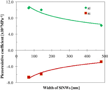
Figure 8 With dependence of piezoresistive coefficients in 〈 110 〉 crystallographic direction.
The results show a very large increase in the longitudinal piezoresistive coefficient when the width is smaller than 150 nm. The shear piezoresistive coefficients π44 of the 35 nm SiNW was found to be 260× 10−5 [MPa −1], i.e. around 88% larger than the value reported by Toriyama et al [10], and 100% larger than the value reported by Tufte and Steltzer [11]. The shear piezoresistive coefficient of the 490 nm SiNWs is 164× 10−5 [MPa −1], which is slightly higher than the values reported in [10, 11] for the same impurity concentration of 1.2× 10¹⁸ atoms cm −3 (figure 9).
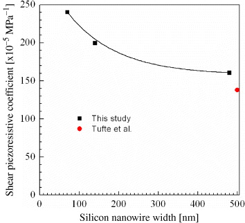
Figure 9 Shear piezoresistive coefficient π 44.
However, there is still a big difference between the measured and theoretical values due to the difference in the nanowire's width in the calculation (several nanometers) and in experiment (several tens of nanometers). Therefore, further theoretical and experimental studies of the piezoresistive effect in SiNW are necessary to eliminate this difference.
4. Piezoresistive effect of CNT thin film deposited on a MEMS structure
Research on carbon nanotubes (CNTs) for sensing application is a very promising direction for nanoscale devices due to CNTs' excellent electrical and mechanical properties. In addition to the characteristics of either a metallic conductor or a semiconductor, which allow CNTs to become promising components of integrated circuits to continue shrink the transistor size, CNTs possess a tensile strength larger than any other known materials [12]. CNTs have been studied for various applications, such as tunable electrometrical oscillators, chemical and physical sensors, non-volatile memory and actuators.
The integration of CNTs into a MEMS structure usually relies either on bottom-up (in-situ growth) or top-down (post-growth) methods. The bottom-up technique utilizes catalytic particles directly patterned on a substrate to control the position of CNTs, while the top-down method focuses on manipulation of the growth CNTs to specific positions. Although bottom-up methods have particular advantages in the area of field-effect devices, the poor compatibility with MEMS technology is the main obstacle for MEMS integration and functional devices. In order to be effectively applied to MEMS devices, CNTs should have well-controlled properties and orientation, and be easily integrated into the system. An alternative and probably more realistic approach is to assemble a large CNT film at desired locations and pattern it by conventional top-down lithography. A recent approach was reported by Hayamizu et al [13]. This highly efficient process is known as 'super growth'. The 'super growth' CNTs have high purity and millimeter-scale length. Therefore, the top-down technique can be used to integrate CNTs onto microstructures. This process allows complex CNT components for integrated devices and, therefore, potentially opens a way for low-cost CNT-based MEMS devices.
One of the prominent sensing properties of CNTs is the piezoresistive effect. This effect was investigated for the first time by Tombler et al [14]. A gauge factor (the CNTs' sensitivity to strain) of 1000, i.e. five times larger than that of single crystal silicon, was reported. Other measurement of Cao et al [15] showed a gauge factor of up to 3000 for pre-strained individual SWNTs. This paper reports on the integration of CNT film into a MEMS structure and the characterization of piezoresistive coefficients of integrated CNT elements. The test specimen was made of aligned single wall carbon nanotube (SWCNT) forest films, which are possible for top-down process.
4.1. Integration of CNT film on a microstructure
CNTs have been synthesized by water-assisted chemical vapor deposition (CVD), a process known as 'super growth' [16]. Super growth CNTs are catalyst-free SWCNTs with a diameter of 2.8 nm, carbon purity higher than 99.9%, vertically aligned, a length in millimeter-scale, and occupying 3–4% of the total volume of this forest film. Self-assembled SWNTs were vertical aligned in the form of sparse forest films and then zipped into high density SWNT films by the liquid induced zippering effect. After positioning the film onto the prefabricated silicon device, lithography was performed to pattern the film into the desired shapes. The integration of CNT film into microstructures is shown in figure 10. 500×500×4 μm 3 (L×W×T) CNT films were first synthesized by water-assisted CVD (figure 10(a)). 0.3 μm Cr/Au electrodes were created by the lift-off process on a silicon wafer with a passivation layer (Si 3 N 4) on top (figures 10(c) and (d)). Thanks to the large size of the forest film, the CNT film was manually placed on the electrodes within isopropyl alcohol (IPA) solution and dried naturally. The surface tension of the solution and strong van der Waals interaction accordingly compressed the CNT film into a 0.3 μm thick layer and formed a strong contact with the electrodes (figure 10(e)). Once densified, the SWNT film could be considered as a continuous material layer. A hydrogen silsesquioxane (HSQ) resist was spin-coated and baked at 90 °C for 10 min. HSQ was then patterned by EB lithography and developed by tetramethylammoniumhydroxide (TMAH) solution (2.38%, ZTMA—100, Zeon) (figure 10(f)). Then, the CNT film was etched by reactive ion etching (RIE) (RIE-200L, Samco) with oxygen plasma and argon to define the designed shape (figure 10(g)). The HSQ mask was finally removed by buffered hydrofluoric acid (figure 10(h)). Figure 11 shows SEM images of the CNT thin film elements as strain gauges [17].
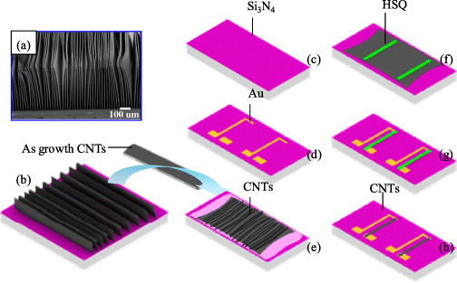
Figure 10 Integration process of CNT film onto a microstructure. Super-growth synthesized CNT ((a), [16]).
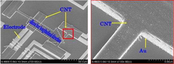
Figure 11 SEM image of integrated CNT elements.
To measure the piezoresistive effect, CNT elements were patterned onto a silicon bar with dimensions of 50×5×0.5 mm 3, and the bar was bent by the four-point bending method. The 40×5×0.3 μm 3 CNT elements were aligned in either the longitudinal or the transverse direction of the bar and connected by Cr/Au interconnection to facilitate four-point probe measurement, which eliminates unexpected contact resistance. The resistance of the CNT elements was measured to be 3.04 kΩ and 124.14 kΩ, corresponding to the parallel and perpendicular CNT directions, respectively. The I–V characteristic was linear and repeatable during the measurement. Figure 12 shows the relation between the relative change of resistance ΔR/R versus strain applied to the CNT film [17]. The longitudinal and transverse gauge factors, measured when the CNT was aligned with the longitudinal stress direction, were G L =6.24 and G T =0.67. With Young's modulus of CNT film 9.7 GPa, as reported in previous work [13], the piezoresistive coefficients were calculated to be π L =81.9×10⁻⁵ MPa −1 and π T =7.37×10⁻⁵ MPa -1, respectively.
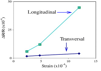
Figure 12 Relative change of resistance versus strain.
Although the piezoresistive coefficient is two times that of bulk silicon, the current testing showed that SWCNT film did not possess giant effects as reported for individual SWCNTs. The main reason could be that the CNT bundle was embedded in the film. The bundles change their resistances during the bending test by contact resistance and by elongating CNT bridges, and also due to tunneling contact between the nanotubes. Thus, a higher piezoresistive effect would be expected with smaller, well aligned CNT film.
5. Piezo-optical effect in a photonic crystal nano cavity
A photonic crystal (PhC) is a periodic nanostructure of materials with a high contrast refractive index such as silicon and air. PhCs possess a variety of band dispersions and band gaps, where the propagation of light is prohibited for certain ranges of wavelength. By choosing different materials and geometrical parameters, the propagation of light can be modified in many ways and, therefore, Si PhC-based devices have been widely used in light control applications, such as waveguides, photonic band gap structures and resonators [18]. Moreover, because of their sensitivity to small refractive index changes, PhC structures have been studied for biochemical sensing by detecting the change in refractive index due to molecule immobilization in PhC [19, 20]. Recently, a study of the mechanical sensing effect of PhCs has attracted a lot of attention due to its high-resolution strain sensing possibilities [21–23].
The piezo-optic effect can be defined as the change in optical properties of the PhC structure upon application of a mechanical stress/strain. In order to evaluate the piezo-optic effect, we will investigate the shift in resonant wavelength of the PhC nanocavity upon application of mechanical stress/strain. The detection of the shift in wavelength is chosen due to the lower sensitivity to background noise, which usually affects the signal level. The PhC nanocavity used in this study is created by missing a circle of air holes of a triangular lattice PhC, as shown in figure 13. The hole radius, r, is 0.38a (where a=420 nm is the lattice constant).
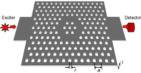
Figure 13 Schematic of a 2D PhC nanocavity: a=420 nm, r=180 nm, t=220 nm, r/a=0.38.
The change in PhC geometry upon mechanical stress/strain is analyzed by using the structural finite element method (FEM), such as ANSYS software. Figures 14(a) and (c) depict the simulated deformation and relocation of an airhole lattice under longitudinal and transverse strains.
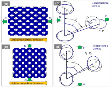
Figure 14 Deformation and relocation of an airhole lattice of PhC structure under applied strain.
Next, the geometric change is then input into a Finite Difference Time Domain (FDTD) simulation to simulate the light transmission spectrum of the PhC nanocavity. The effective refractive index of air/220 nm-Si/air is calculated to be 2.81. The analysis performed in this work used TE polarization light (i.e. the electric field component parallel to the PhC plane).
Both tensile and compressive strains have been applied and investigated in this study. Figure 15 shows the transmission spectra of the PhC cavity corresponding to different applied strains. Figure 16 shows the linear relations of resonant wavelength shift versus longitudinal and transverse strains. The wavelength shift was 1.9 nm mε−1 for longitudinal strains, about 2 times larger than that reported by Lee and Thillaigovindan [22].

Figure 15 Transmission spectra show resonant wavelength under different strains.
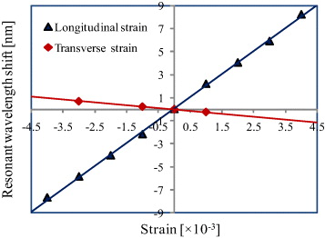
Figure 16 Resonate wavelength shift versus strain.
With the minimum detectable wavelength of the present commercial optical spectrum analyzer (e.g. Agilent-83453B-HRS) being 0.008 pm, we can obtain the minimum detectable strain of 5.3×10⁻⁹, i.e. the smallest detectable strain known to the authors.
6. Conclusion
In this paper, we have presented a theoretical analysis of the electronic state of silicon nanostructures based on first-principles calculation. The results show very different energy band structures, i.e. direct band gap compared to indirect band gap of the bulk silicon, due to the quantum confinement effect. These differences affected the electrical and optical properties and, therefore, would influence the piezoresistive effects in nanostructures. This assumption was then experimentally verified for the case of SiNW, and we found that the smaller the SiNW, the higher the piezoresistive coefficient. However, the measurement values were still much smaller than the simulation values. This is due to the difference in width of the SiNW between the simulation and measurement model. Therefore, further experimental investigation for smaller SiNWs, e.g. below 20 nm width, is necessary. We also reported the integration and patterning methods of SWCNT film on a MEMS structure, as well as measurement of the piezoresistive effect of the SWCNT film. The longitudinal piezoresistive coefficient of the SWCNT film was two times higher than that of the bulk silicon. This is promising for CNT-based highly sensitive mechanical sensors. Finally, theoretical analysis of the piezo-optical effect in a PhC nanocavity showed extremely high resolution strain sensing, i.e. the smallest detectable strain might be down to nano strain. These achievements, including the nanofabrication of typical nanostructures and evaluation of their piezo-effects, would be significant in developing highly sensitive and high resolution mechanical sensing devices based on nanostructured materials.
Acknowledgments
This study was partly supported by the Ministry of Education, Culture, Sports, Science and Technology of Japan under the Grant-in-Aid for Young Scientists (No. 21710141-0001).