
Abstract
We review the information that we have obtained from combined Raman spectroscopy and electron diffraction experiments on individual free-standing single-walled carbon nanotubes (SWNT). From these data, we define Raman criteria allowing the indexing of SWNTs from their Raman features only and we show the efficiency of this approach in assigning the structure of individual carbon nanotubes. These results on index-identified individual SWNTs are compared with theoretical predictions.
Export citation and abstract BibTeX RIS

Content from this work may be used under the terms of the Creative Commons Attribution-NonCommercial-ShareAlike 3.0 licence. Any further distribution of this work must maintain attribution to the author(s) and the title of the work, journal citation and DOI.
1. Introduction
The structure of a single-walled carbon nanotube (SWNT) is uniquely described by the pair of integers (n, m) that refer to the number of a1 and a2 unit vectors of the graphene lattice that are contained in the chiral vector, Ch =n a1 +m a2 , that spans the circumference of each nanotube [1]. SWNTs are classified as chiral (0<m<n) and achiral (m=0 or n=m), which in turn are known as zigzag (m=0) or armchair (n=m) SWNTs. The best and unambiguous way to determine the structure of an SWNT, and then the (n, m) indices, is to measure its electron diffraction pattern. To perform electron diffraction, each individual SWNT has to be free-standing [2].
Knowledge of the (n, m) indices is also crucial to the nanotube electronic structure. Specifically, SWNTs for which |n−m|=3q are metallic and those for |n−m|=3q±1 are semiconducting, where q is an integer.
Regarding the optical properties, each SWNT (n, m) has a unique set of interband transitions, E ii , denoting the energy differences between the ith van Hove singularities in the conduction and valence bands for semiconducting (E S ii ) and metallic (E M ii ) SWNTs. E ii values consist of one-particle energies and many-body corrections, which are decomposed into an exciton bending energy and a self-energy. The lowest-order transitions (E S 11, E S 22, E S 33, E S 44 and E M 11, E M 22) fall in the visible and near infrared regions depending on the tube diameter. Calculation of these transitions for all (n, m) leads to the so-called Kataura plot in which the energies of the different transitions are plotted as a function of the tube diameter [3].
In 2005, an important breakthrough in carbon nanotube research was the first observation of Raman spectra from individual index-identified free-standing SWNTs [4]. The measurement of the Raman spectrum from one individual SWNT is possible because of the very large density of electronic states close to the van Hove singularities of this one-dimensional structure. Consequently, when an incident or scattered photon matches an electronic transition (resonance condition), the Raman signal exhibits a large enhancement. This resonance condition has to be fulfilled to observe a Raman signal of an individual free-standing SWNT [4–6].
In this context, we have developed an approach combining resonant Raman spectroscopy (RRS) and electron diffraction (ED) experiments on individual, spatially isolated, free-standing SWNTs. This approach allows us to measure, in air and room temperature, the RBM [4] and the G-mode features [5], as well as to evaluate with good accuracy the transition energies of a few individual semiconducting and metallic index-identified free-standing SWNTs [7, 8]. From this approach, we have been able (i) to determine the intrinsic dependence of phonons on diameter and chirality and (ii) to define Raman criteria allowing the identification of the structure of free-standing SWNTs from their Raman features only. In this review, these criteria are reported and used to (n, m)-assign individual SWNTs. The experimental Raman results are compared with theoretical predictions. In particular, we confirm that non-adiabatic effects have to be taken into account to describe accurately the phonons of metallic SWNTs.
2. Results
Radial breathing mode (RBM) and G-modes are the two main features of the first-order Raman spectrum of an SWNT (figure 1). The // // polarized Raman spectrum of a chiral semiconducting and a chiral metallic SWNT are displayed in figure 1 (// // means that the incident laser and scattered light polarizations are along the tube axis).
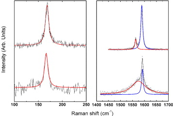
Figure 1 The Raman spectrum of a (11, 10) semiconducting SWNT (top) and a (15, 6) metallic SWNT (bottom). RBM (left) and G-modes (right).
2.1. RBM frequency versus diameter relationship
The low-frequency mode of each previous Raman spectrum is assigned as the radial breathing mode (RBM) of the nanotube under consideration. The measurements of the RBM frequency of five semiconducting ((11, 10), (17, 9), (15, 14), (27, 4) and (23, 21)) and six metallic ((10, 10), (16, 4), (15, 6), (13, 10), (16, 7) and (12, 12)) individual free-standing index-identified SWNTs [4, 5, 9] led to the following RBM frequency versus diameter relationship (figure 2),

In this relation, the diameter d is given from the knowledge of the (n, m) indices by the expression [1] , where a C–C =0.142 nm.
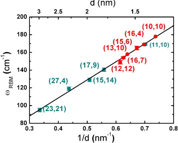
Figure 2 RBM frequency versus inverse diameter for 11 (n, m) SWNTs index identified by electron diffraction (dots). The solid line is a fit of the data from equation (
This experimental relation, established independently from any modelization for SWNTs in the diameter range 1.35–3 nm, is valid within ±1 cm −1 for free-standing SWNTs measured in air and at room temperature. The constant additional factor in the RBM frequency versus the inverse diameter is supposedly associated with environmental effects and then is expected to be weak for negligible environmental effects. Opposite to this prediction, a relatively large constant factor, 27 cm −1, is found in experiments on free-standing SWNTs for which environmental effects are supposed to be weak. However, as recently suggested [10], the constant additional term in this expression can be understood as due to the interaction between the free-standing SWNT and the surrounding air. Room temperature Raman experiments on individual free-standing SWNTs under high vaccum, and after thermal annealing at high temperature, are in progress to highlight this point. In the following, we use the relation 1 to derive the diameters of in air free-standing SWNTs from the precise measurement of their RBM frequencies.
2.2. G-modes
Another criterion to identify the SWNTs' structure is the number of G-modes which appear in the // // polarized Raman spectrum. This number is completely determined from symmetry considerations (for a review see [11] and references therein). As shown, for instance, in [12], only both modes, LO and TO G-modes, belonging on A1 symmetry, are active in the // // Raman spectrum of a chiral SWNT. By contrast, a single component of A 1g symmetry, LO for metallic and semiconducting zigzag nanotubes and TO for metallic armchair tubes, is active in the Raman spectrum of an achiral SWNT. In other words, the number of G-modes measured in the // // polarized Raman spectrum of a tube under investigation permits the identification of its chiral or achiral character. A number of components greater than two unambiguously identifies the measurement of a bundle or a multi-walled nanotube such as a double- or triple-walled nanotube. In the spectrum of figure 1, in agreement with these symmetry considerations, two G modes are observed for each chiral SWNT and a single component is observed in the Raman spectrum of achiral SWNTs (figure 3).
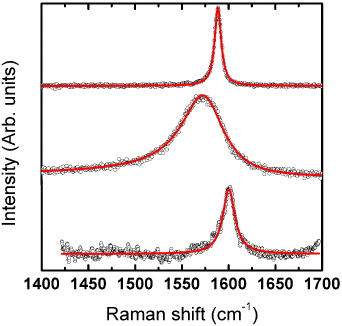
Figure 3 The intrinsic Raman responses in the G-mode range of the three types of achiral SWNT. From top to bottom: semiconducting zigzag (25, 0), metallic zigzag (24, 0) and metallic armchair (10, 10).
The lineshape of the G-band is significantly different for chiral semiconducting compared to metallic SWNTs. Qualitatively, in a chiral semiconducting tube, the profile of each G-mode is narrow and symmetric. The high-frequency mode, typically around 1590 cm −1, is assigned to the longitudinal mode (LO) and the low-frequency mode to the transverse mode (TO). In a chiral metallic tube, a broad low-frequency mode is found and a narrow high-frequency mode is observed, typically around 1590 cm −1. In agreement with theoretical work [13], the high-frequency mode is assigned to the TO mode and the broad low-frequency mode to the LO mode, the opposite of semiconducting nanotubes. In zigzag SWNTs, for which only the LO component is Raman active, a single broad low-frequency band is observed in the zigzag metallic SWNT and a narrow high-frequency line is found in the zigzag semiconducting SWNT (figure 3). In an armchair metallic SWNT, only the TO mode is Raman active and a single narrow high-frequency component is measured (figure 3).
The softening and broadening of the LO component in metallic tubes with respect to that in semiconducting tubes is assigned to a Kohn anomaly at the Γ point of the Brillouin zone related to a real electron–hole pair created by a phonon excitation process [13]. In terms of characterization, the lineshape of the low-frequency component clearly identifies the semiconducting or metallic character of the chiral tubes under investigation.
2.3. Optical transitions
The measurement of the complete Raman spectrum (RBM and G-modes) of an individual SWNT is only possible if the excitation laser energy used in the experiment is in resonance or quasi-resonance with one of the transition energies of the tube under investigation. In consequence, this resonance condition allows us to evaluate with good accuracy the transition energies of a few index-identified individual SWNTs. These results have been used to normalize calculations of the transition energies carried out by using a non-orthogonal tight binding approach [14] leading to the normalized Kataura plot in figure 4. This normalized Kataura plot is the key for the (n, m)-assignment of SWNTs from Raman spectroscopy.
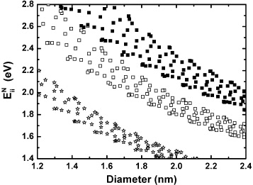
Figure 4 The normalized Kataura plot. E M 11 transition (black stars), E S 33 transition (black open squares) and E S 44 transition (filled squares).
2.4. Methodology
The procedure to identify SWNTs is as follows. From the measurement at a given excitation energy (E laser ) of the complete Raman spectrum (RBM and G-modes) of a tube, we can evaluate its diameter from the RBM frequency versus diameter relationship. The lineshape of the G-modes permits us to identify the metallic or semiconducting character as well as the chiral or achiral type of the tube under investigation. Combined with the laser excitation, this information allows us to determine the order of the transition involved in the Raman process. By reporting on the normalized Kataura plot, the couple (diameter, E laser ), we can assign from comparison the (n, m) structure of the tube investigated. The success of this approach will be illustrated by some examples in the next section. Obviously, to determine unambiguously the (n, m) indices of an SWNT, all of the criteria discussed above must be fitted together and if one of them is not consistent with the others, the tube investigated is in a bundle or doped, or it is a multi-walled nanotube (MWNT).
2.5. Identification of individual free-standing SWNTs
We show in figure 5(a) the Raman spectrum of a nanotube in resonance with a 2.41 eV excitation energy. A single RBM is located at 174.6 cm −1, giving a diameter of 1.38 nm for this SWNT. The G-mode lineshape is that of a chiral semiconducting nanotube with two narrow components located at 1563 cm −1 (TO) and 1590 cm −1 (LO), respectively. Because the RBM and G-modes were detected at the 2.41 eV excitation, the optical transition of the semiconducting tube under investigation is very close to 2.41 eV. Regarding the diameter of this semiconducting tube (1.38 nm), the involved transition is the third excitonic transition, E S 33. The diameter and the 2.41 eV laser energy are reported on our normalized Kataura (red triangle in figure 5(a)). A good match between these features and those of the (12, 8) tube (blue dot in figure 5(a)) is found, leading us to identify unambiguously the tube under investigation as the (12, 8) SWNT. A careful examination of this region of the Kataura plot rules out other (n, m)-assignments.
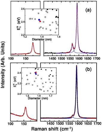
Figure 5 (a) RBM (left) and G-mode (right) ranges of the Raman spectrum of an individual freestanding SWNT in resonance at 2.41 eV. Inset: zoom of the normalized Kataura plot. Open and filled squares are for calculations of the third and fourth transitions of the semiconducting tubes, respectively. The red triangle is the (1.38 nm, 2.41 eV) experimental couple. The blue dot is the calculated E S 33 energy transition for the (12, 8) SWNT. (b) RBM and G-mode ranges of the Raman spectrum of an individual free-standing SWNT in resonance at 2.41 eV. Inset: zoom of the normalized Kataura plot. Open and filled black squares are for calculation of the third and fourth transitions of the semiconducting tubes, respectively. The red triangle is related to the (1.57 nm, 2.41 eV) experimental couple and the blue dots are the calculated energy E S 33 transition for the (20, 0) and (19, 2) SWNTs.
Another example is shown in figure 5(b), where the Raman spectrum of a nanotube in resonance with the 2.41 eV excitation energy is displayed. A single RBM is located at 157 cm −1, giving a diameter of 1.57 nm for this SWNT. The G-mode lineshape is the one of a chiral semiconducting nanotube with two narrow components located at 1570 cm −1 (TO) and 1590 cm −1 (LO), respectively. The weak intensity of the TO mode indicates that the tube under investigation is a low-chiral angle SWNT. Regarding the diameter of this semiconducting tube (1.57 nm), the involved transition, close to 2.41 eV, is the third excitonic transition. The couple (1.57 nm, 2.41 eV) is reported on our normalized Kataura (red triangle in figure 5(b) (inset)). A good match between these features and those of the (20, 0) and (19, 2) tube (blue dots in the inset of figure 5(b)) is found. Due to observation of two components in the G-mode range of the Raman spectrum, the assignment of this tube as the zigzag (20, 0) SWNT is ruled out. In consequence, the tube under investigation here is assigned as the (19, 2) SWNT.
It must be remembered that if one of the previous criteria is not consistent with the others, one can conclude that the tube investigated is in a bundle or doped, or is a multi-walled nanotube (a DWNT, for instance). The following result illustrates this statement. The RBM and G-mode ranges of the Raman spectrum on a free-standing tube measured at a 1.96 eV excitation energy are displayed in figure 6. The RBM is located at 123.5 cm −1, leading to a diameter of 2.11 nm. The G-mode profile is typical for a chiral semiconducting SWNT (see figure 1). The diameter and the 1.96 eV laser energy, close to the transition energy of the tube under investigation, are reported on the normalized Kataura (red triangle in figure 6 (inset)). The experimental feature falls in the gap between the third (open squares) and fourth (filled squares) transitions of semiconducting SWNTs. Consequently, the tube under investigation cannot be identified as an individual SWNT. However, it has been found from Raman [6, 15] and Rayleigh [16] experiments carried out on individual tubes and thin bundles that the interaction between the tubes in a bundle red shifts the transition energies of SWNTs compared to their individual form by a value around 50–100 meV. Consequently, a possible assignment of the tube under investigation here could be the (22, 8) SWNT in a bundle with non-identified (and non-resonant at the 1.96 eV excitation energy) SWNTs. The arguments in favour of this assignment are the close value of the calculated and experimental diameters, 2.107 nm and 2.11 nm, respectively; and the 90 meV redshift between the calculated energy of the (22, 8) SWNTs and the experimental resonance energy, 2.052 eV and 1.96 eV, respectively.
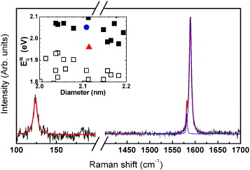
Figure 6 RBM and G-mode ranges of the Raman spectrum of an individual tube in resonance at 1.96 eV. Inset: zoom of the normalized Kataura plot. Open and filled squares are for calculations of the third and fourth transitions of semiconducting tubes, respectively. The red triangle is the (2.11 nm, 1.96 eV) experimental couple. The blue dot is the calculated energy transition for the (22, 8) SWNT.
2.6. Diameter dependence of the G-mode frequencies
In figure 7 are reported the diameter dependence of the frequency of the TO G-mode measured from semiconducting SWNTs (figure 7, top) and that of the LO G-mode measured from metallic SWNTs (figure 7, bottom). All of the tubes have been identified from electron diffraction or from our Raman criteria.
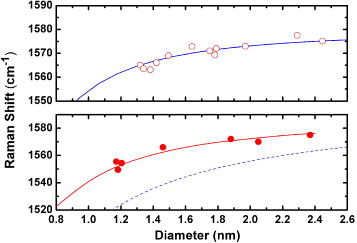
Figure 7 Top: diameter dependence of the frequency of the TO component of the G-band for semiconducting SWNTs. Experimental (red open dots), calculated in an adiabatic approach (blue solid line). Bottom: diameter dependence of the frequencies of the LO G-mode of metallic SWNTs. Experimental (red filled dots), calculated in a non-adiabatic (red solid lines) and an adiabatic (blue dashed lines) approach (from [13]).
In the diameter range investigated, the experimental TO G-mode frequency for metallic SWNTs and LO G-mode for semiconducting SWNTs (located around 1590 cm −1, not shown) slightly depends on the diameter [5, 8], as predicted theoretically [13]. By contrast, the LO G-mode frequency for metallic SWNTs and TO G-mode for semiconducting SWNTs display a significant diameter dependence (figure 7). The experimental data are compared with the calculations performed in the framework of adiabatic and non-adiabatic approaches [13]. For semiconducting, the dependence of the TO G-mode frequency is well described in an adiabatic approach. By contrast, a better agreement between the experimental and calculated LO frequencies for metallic SWNTs is found when calculations are performed in a non-adiabatic model [13]. These experimental findings obtained on index identified metallic SWNTs definitively support the fact that both curvature and non-adiabatic effects have to be taken into account to correctly describe the LO G-mode frequencies for metallic SWNTs. Indeed, in the framework of an adiabatic approach, the calculated frequencies of the LO modes are significantly downshifted (about 20 cm −1) in the diameter range investigated (figure 7, dashed line). The agreement between experiments and predictions also justifies a posteriori the identification from our Raman criteria of free-standing SWNTs.
3. Conclusion
Based on combined Raman and electron diffraction experiment data, we have determined several Raman criteria that allow the Raman identification of semiconducting and metallic free-standing SWNTs at room temperature and in air. In the framework of this approach, we have reported the (n, m) identification of individual free-standing SWNTs. From an example, we have illustrated the following statement: if one of the criteria is not consistent with the other ones, it means that the tube investigated is not an individual SWNT. This study emphasizes the ability and difficulties of resonant Raman spectroscopy as a metrological method for the characterization of carbon nanotubes. Finally, concerning metallic SWNTs, our measurements support the description of the dynamics of the G-mode in a non-adiabatic theory.
Acknowledgments
The authors thank R Arenal, S Piscanec, L Henrard and V N Popov for support and helpful discussions. This work has been done within the framework of the GDR-E No 2756 'Science and Application of the Nanotubes-NANO-E'. The authors acknowledge financial support from the ANR project ExciTubes.