
Abstract
Miniaturization of sensitive magnetic sensors for nano- and picosatellites has come to the point where the traditional sensors with magnetic coils can soon be replaced. Thin film technology offers the possibility of making extremely small magnetic field sensors that employ the effect of anisotropic, giant and tunnelling magnetoresistance (AMR, GMR and TMR). In this paper, the development status of sensors based on microelectromechanical systems technology (MEMS), starting from a TMR layer structure, is presented. The sensors have been successfully fabricated and integrated onto an electronic circuit designed for space application. The system as a whole and the sensors in particular have not only been characterized with respect to sensitivity, resolution and noise level but also to launch vibration and space radiation. The sensor performance and limitations are strongly dependent on the deposited materials, sensor design and fabrication process. Since the sensor elements are small and sensitive (with lateral dimensions of some tens of micrometres and resolution of 100 pT at frequencies of MHz), they are also promising for other MEMS applications.
Export citation and abstract BibTeX RIS

Content from this work may be used under the terms of the Creative Commons Attribution-NonCommercial-ShareAlike 3.0 licence. Any further distribution of this work must maintain attribution to the author(s) and the title of the work, journal citation and DOI.
1. Introduction
The traditional magnetic sensors that employ coils (search coil, fluxgate) or vaporized material (SERF), or which require a low temperature (Squid), offer very high performance but are difficult to miniaturize. A different physical sensor principle is required to reach another size regime, and shift the dimension and mass, respectively, from cubic decimetres to cubic centimetres, and kilograms to grams. Solid state magnetic sensors, such as Hall sensors, or those employing AMR, GMR and TMR, can do this employing micro- or nanoelectromechanical system (MEMS and NEMS) technology. Indeed, the thin films that make up the actual sensor elements have a thickness of some nanometres to some micrometres, whereas the substrate is usually two to three orders of magnitude thicker. However, the much larger and bulkier substrate will remain necessary unless the thin film sensor elements can be integrated into, e.g. their supporting electronic system.
The motivation for heavy miniaturization stems not only from the reduction of production costs by using MEMS batch processes but also from the desire for increased performance and reduced power consumption. The decreased size and mass are themselves important aspects for space applications, as the launch cost can be reduced. Because of this, new satellite classes, so-called nano- and picosatellites, have been established. These satellites, by definition, are less than 10 kg and 1 kg, respectively, in total mass. Thus, their mass, volume and power budgets are very limited. Despite this, the aim is to maintain a high functionality for them—sometimes comparable with that of full-size satellites.
The work presented in this paper deals with a magnetic sensor employing the TMR effect. The design and fabrication issues governing sensor performance are also discussed.
2. Background
For the needs of iterative design and time saving fabrication, tailored rapid prototyping methods were developed. The first of them used a focused ion beam (FIB) to pattern magnetic tunnel junctions (MTJs) from a so-called tunnel magnetoresistive (TMR) layer structure [1, 2]. The method proved to be time effective but mostly suitable for quick feasibility studies unless the implantation of Ga ions in the MTJ layers, which reduces the magnetoresistance and changes the coercivity, could be tolerated or circumvented.
Having established the function of the TMR material system, another method was needed to pattern the MTJs with good enough performance. Here, a second rapid prototyping method, using an electron spectroscopy for chemical analysis (ESCA) system, was developed [2]. An ESCA system is built for material analysis and is usually equipped with an Ar ion gun for depth profiling by intermittent sputtering. Here, the ion gun was used for a gentle patterning of MTJs. The ESCA system also offers the possibility of stopping the physical etching process with very high accuracy. This makes it possible to fabricate MTJs with different electrodes (the sensing and reference layers in this case) in terms of size and shape, and, hence, enables an interesting investigation of, for example, size versus performance.
TMR sensors are known to have good performance over a broad frequency band (from some hundred Hz to GHz) with a very low noise floor. For many applications, such as for space and medicine, frequencies from dc to kHz are of particular interest. According to an empirical expression [3], the low-frequency noise, Sv , of an MTJ depends on the bias current, I b , the resistance, R, the area, A, the modified Hooge parameter, α H and the frequency, f, according to

Hence, for a given TMR layer stack, the MTJ area is obviously a most interesting design parameter. A large area should lead to low noise in the MTJs, but it also gives rise to a low resistance of the MTJs that may affect their TMR ratio. A design optimization was therefore needed. Two experimental series were therefore conducted: patterning and characterizing of circular MTJs with different diameters, and patterning and characterizing of MTJs with different electrodes.
3. Materials and methods
The initial material for patterning the MTJ was a TMR layer stack sputtered on a thermally oxidized Si (100) wafer. From the top, the layers were 7 Ru/10 Ta/3 Co60Fe20B20/0.3 Mg/1.1 MgO/3 Co60Fe20B20/0.8 Ru/2.5 Co70Fe30/20 PtMn/5 Ta/30 CuN/5 Ta, where the large numbers are thicknesses in nm and subscripts are contents in at.% (the PtMn was nominally equiatomic). The stack was fabricated by Singulus Technologies AG, Germany, and is the same as the one in [1].
Since the physical etching in the ESCA system was rather slow, and the scanned area on the sample was only 4×4 mm, the sample of 10×10 mm was pre-patterned in a broad Ar ion beam facility (Sputnik, Albanova Nanofabrication Facility, Sweden). In this process, the bottom contacts were etched into 200×50 μm rectangles. The etch mask was made by photolithographic patterning of a 150 nm thick aluminium film deposited by magnetron sputtering (CS 730S, von Ardenne, Germany) in an 800 W Ar plasma under a process pressure of 0.44 Pa.
The patterning process to make circular MTJs was continued in the ESCA system (PHI Quantum 2000, Physical Electronics, USA) after standard lithography. The ion gun of the ESCA system was at an angle of 45° to the sample surface, and the sample was rotated to receive a uniform etch dose (figure 1). Thus, the diameters of the MTJ top and bottom electrodes were slightly different, and depended on the ion beam angle, the thickness of the photoresist mask and the thickness of the TMR stack.
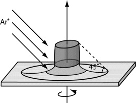
Figure 1 Configuration of the ion beam and the sample in the ESCA.
The process steps for patterning the pre-patterned rectangles into MTJs were roughly the same as described in [1]. Figure 2 shows the sensor element design and a fabricated MTJ. Note that the fabricated MTJ has not yet received its electric contacts.
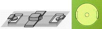
Figure 2 Schematic MTJ (left), and fabricated MTJ (right).
In the first experiment series, Series A, the MTJs were patterned in the ESCA system through the layer stack and the etch process was stopped almost at the bottom of the antiferromagnetic layer PtMn. (A denotes the etch stop at the antiferromagnetic layer.) In the second experiment series, Series B, the patterning process was stopped at the 1-nm thin tunnel barrier of MgO (similarly, B denotes the etch stop at the barrier), leaving the synthetic antiferromagnetic (SAF) structure, i.e. the layers beneath the barrier, unchanged, i.e. in the shape resulting from the pre-patterning process. Thus, the bottom electrodes were much larger than the top electrodes. The precise etch stop was possible because the gentle etch steps could be performed sequentially with the steps of material analysis in the ESCA system.
In order to investigate the quality of the MTJ patterning process in the ESCA system, an examination using transmission electron microscopy (TEM) was performed. A sample for TEM was prepared from an MTJ from Series B using a FIB system (Strata DB235, FEI Company, USA). To avoid Ga implantation into the layer stack, the MTJ was protected by a Pt layer deposited by both electron- and ion-assisted chemical vapour deposition (EA- and IA-CVD) in the FIB system before the actual milling and thinning of the sample.
The patterned MTJs were characterized with respect to their resistance and noise level. For measurement of the resistance as a function of the applied magnetic field, a four-point voltage probe (Keithley 2182, Keithley Instruments Inc, USA) and an electromagnet were used. The field was swept between ±25 mT and the resistance was calculated from the bias current of ±5 mA applied to the sensor. This alternating bias current was needed to remove the contact voltage. For noise measurements, the bias current was steadily kept to 5 mA and the noise signal was amplified at 60 dB using a low noise amplifier (Model565, HMS electronics, Germany), which had a inherent noise of around . The data were sampled by a spectrum analyser (HP 35670A, Hewlett Packard, USA). To minimize the current noise, lead acid accumulators were used for biasing both the MTJs and the amplifier. All MTJs and batteries, and the amplifier, were placed in two mu-metal boxes to shield them from external noise sources. The low-frequency noise of the MTJs was measured in two intervals (0.25–400 Hz and 8–12 800 Hz) and was then combined and post-processed by Matlab (R2007a, The Mathworks Inc., USA).
For the purpose of using the magnetometer in space, its MTJs were radiation tested. Here, a total ionizing dose (TID) of 100 krad, a typical requirement for satellite instruments for five year interplanetary missions, was used. The gamma radiation source was Co-60 and a bare MTJ was exposed for the TID. The resistance loop and noise spectrum of the MTJ were measured both before and after the radiation exposure. No relaxation annealing was performed on the MTJs.
Also of relevance for a space application, the fully developed sensor for 3D magnetic field measurement, after integration onto its supporting electronic circuit, was exposed to vibrations with acoustic frequencies according to the qualification test for the Arianne 5 launcher and worse (table 1).
Table 1. Conditions of the five vibration tests conducted.
| 1 | 16–60 Hz | 10 g | 4 min |
| 2 | 60–200 Hz | 22.5 g | 4 min |
| 3 | 200–2000 Hz | 10 g | 4 min |
| 4* | 2000 Hz | 20 g | 1 min |
| 5* | 200 Hz | 50 g | 1 min |
4. Results and discussion
The physical etching process in the ESCA system, especially when resulting in a tilted sidewall of the MTJs, gave rise to a question concerning re-deposition of the materials on the sidewalls possibly causing short-circuiting of the electrodes. It was also important to confirm the precision of the etch stop at the barrier. The TEM image to the left in figure 3 is taken from a Series B MTJ and shows a slope of the MTJ sidewall going from the left to the right. The right image, taken safely away from the slope, shows that the etch process did stop at the MgO barrier. As also seen in the left image, and in a magnified part of the slope, there are signs of material re-deposition. Energy Dispersive Spectroscopy (EDS) could be used to analyse what materials were re-deposited. Awaiting this, a discussion of the effect of the re-deposited materials on the MTJ performance is difficult to carry out. However, analysis of the MTJ performance, presented later in this section, will shed some light on this matter.
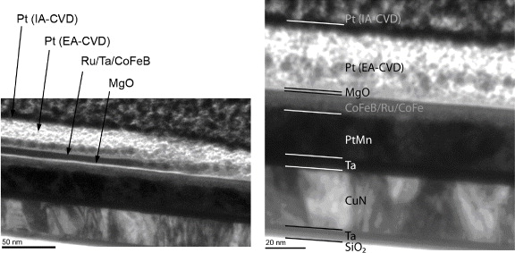
Figure 3 TEM images of a sample from Series B.
To study the relation between resistance and area of the MTJs, samples from experiment Series A were used, and TMR loops of the circular MTJs of different diameters were acquired. Figure 4 (left diagram) shows that the resistance of the MTJs decreased with an increase in their area. For the TMR ratio (figure 4, right diagram), no clear dependency on the areas could be confirmed. This suggests an advantage of using small MTJs.
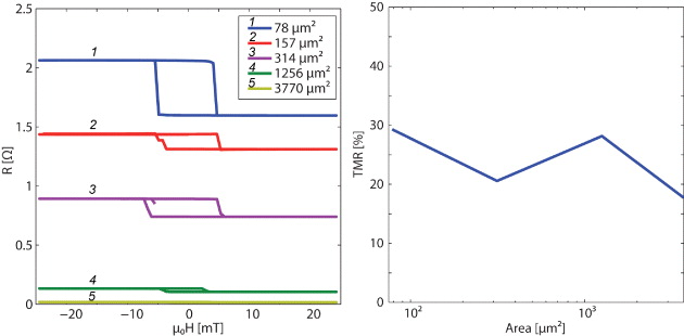
Figure 4 TMR loops of circular MTJs of different size (left), and their TMR ratio as a function of area (right).
On the other hand, the MTJs with larger areas (also from Series A) exhibited lower low-frequency noise (figure 5). The striving for high resistance and low noise of the MTJs was somewhat complicated by the fact that the inherent noise of the signal amplifier set the noise floor for the system. A high sensor noise would of course drown the weak signal to be measured, but if the sensor noise was lower than that of the amplifier, the tiny signal would be at least partly lost between the two noise levels. Further discussion of noise optimization for the system is beyond the scope of this paper. However, matching the noise level of the sensors to that of the amplifier was found to be the best solution.
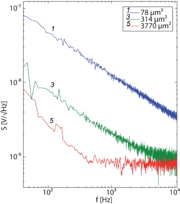
Figure 5 Noise spectrum of MTJs.
To compare the noise levels of the MTJs from Series A and B, three MTJs were studied. Although the etch rate of the ion beam was more or less uniform over the rastered area, the Gaussian shape of the beam made the rims of the area slightly concave. Therefore, from Series B, a MTJ was taken from the middle of the rastered area and another from the region close to the rims (denoted B R ).
The three MTJs studied here did not have the same area. Therefore, their noise figures were normalized to the resistance-area-product (RAP) of the MTJs (figure 6) for comparison. Basically, the low-frequency noise of the MTJs was determined by the modified Hooge parameter, α
H
in equation (
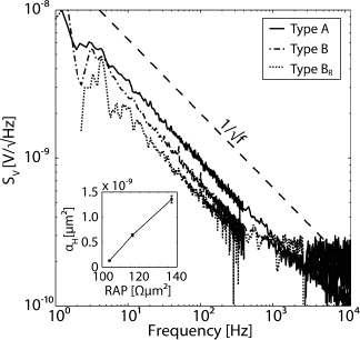
Figure 6 Low-frequency noise of the MTJs with areas normalized to the junction of type A. The inset shows the modified Hooge parameter as a function of the RAP.
The same three MTJs were also studied with respect to magnetic performance. Figure 7 shows the TMR loops of the MTJs of types A, B, and B R measured with a 5 mA bias current. This relatively large current was chosen to give the sensors an intrinsic noise clearly visible above the noise of the amplifier used in the measurement setup of the noise study. The MTJs of type B exhibited higher TMR ratios, of around 45%, than that of the type A, which was around 30%. These figures were consistent with all MTJs in the sample series fabricated, regardless of the diameters (see also the right diagram in figure 4). The lower TMR ratio of type A was assumed to be caused by re-deposited material short-circuiting the barrier. This is supported by the observation of re-deposited material made earlier in the TEM images. The RAP of the MTJs (inset in figure 7) also suggests that the lower TMR and RAP of type A should be caused by the introduction of a TMR-independent conduction channel. Furthermore, although to a lesser extent, the same relations between TMR and RAP for MTJs of type B and B R could be observed. The cause of this for MTJs of type B might be the same, where the barrier was partly etched through, exposing it for the re-deposition problems, whereas the barrier of type B R was intact. The partial etching through the barrier of type B was confirmed in an additional investigation, which is not presented here because of limited space.
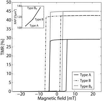
Figure 7 Easy axis TMR loops and RAP (inset) of the studied junctions.
To this point, and without going into a deep analysis of the effects of magnetic domain, shape anisotropy, exchange coupling, and so on, one could say that the MTJs with their top electrode being smaller than their bottom electrode provided a higher TMR ratio and a lower low-frequency noise level. However, this required a precise etch stop at the very thin tunnel barrier. Furthermore, an ad-hoc ion etching system should be able both to fabricate MTJs with vertical sidewalls and to minimize the material re-deposition problem, and thus enhance the performance of the MTJs.
On the effect of radiation on the MTJs, the TMR ratio and noise of a single MTJ were measured before and after radiation with a TID of 100 krad. The negligible change in TMR ratio (figure 8 left) and resistance (not presented in the figure) proved that this dose of gamma radiation did not cause any noticeable change in the magnetic properties of the MTJ. The MTJ showed no noticeable changes in coercivity or magnetostatic coupling, and thus radiation induced charge traps in the MTJ could not be confirmed.
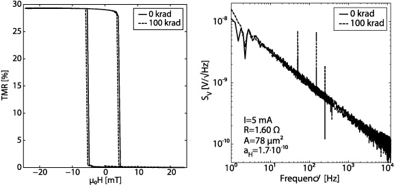
Figure 8 TMR loops and low-frequency noise spectrum of a single MTJ before and after irradiation.
Theoretically, the possible charge traps could still affect the low-frequency noise characteristics of the MTJ, but the measurements conducted before and after irradiation (figure 8 right) did not show any considerable change in the MTJ noise spectrum. The question whether proton and alpha radiation, as also present in space, would have a destructive effect on the MTJs, is still open. However, there are some measures to mitigate the effect, for example creating redundancy by using many MTJs coupled in parallel in a magnetic sensor. The use of a radiation shield of non-magnetic material also ought to be a remedy as long as the mass and volume budget would allow for this. The tiny size of the MTJs is a positive aspect when using MEMS in space, since the probability of being hit by a particle is much lower than for a larger sensor element. However, minimizing the lateral size here will interfere with the noise and resistance of the MTJs, as discussed above, although it is a matter of a circular area with a diameter of one to a few tens of micrometres.
The vibration test for surviving a launch into space would not be meaningful for the MTJs alone as they are solid state sensor elements. Therefore, a sensor system was tested instead. In this system, the sensor elements were connected to the electronic circuit by wire bonding. Aluminium wires with a diameter of 25 μm were used for this. Some wires were left as bonded while other were cast in a two-component epoxy resin (figure 9 right). Not even the two additional tests of table 1 resulted in any damage to the system. A final, fully fledged version of the sensor system for space use could of course employ so called flip-chip mounting, which would eliminate the need for bond wires, although these were proven not sensitive to the vibration, but maybe to the manual handling, and possibly also causing electromagnetic compatibility (EMC) problems. For additional information, the first developed magnetometer was capable of resolving a magnetic signal of about a 100 pT at MHz frequencies.
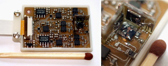
Figure 9 Left: the magnetometer with three orthogonal sensor chips integrated into their supporting electronic circuit for 3D magnetic field measurement. Right: some bond wires were, and others were not, cast in epoxy resin before vibration testing.
5. Conclusions
The effects of material, design, and fabrication process on MTJ performance have been demonstrated. The MTJs with a sensing layer being smaller than the reference layer (here, the top and bottom electrode, respectively) provided a higher TMR ratio and a lower low-frequency noise level. This design required a fabrication process that could be stopped precisely at the very thin tunnel barrier.
It was also demonstrated that an ESCA system can be used for rapid prototyping of MTJs, both for etching through the TMR stack and for etching to the tunnel barrier. The slanted sidewall of the MTJs, being a consequence of the tilted Ar ion beam in the ESCA system, and the material re-deposition on the sidewall had a negative effect on the MTJ performance. However, the fabricated MTJs demonstrated their adequacy for use as elements in a magnetic field sensor.
The size of the MEMS-based MTJs, their sensitivity, and their resistance to radiation and vibration proved promising for use in space. In any case, the low-frequency noise problem with the MTJs must be solved in order to make them competitive to traditional magnetic sensors.
Acknowledgments
This work was supported by the Swedish National Space Board, and the Swedish Governmental Agency for Innovation Systems, VINNOVA. The authors are grateful to doctors J Langer and B Ocker at Singulus AG for providing the TMR layer stacks and Lennart Åhlen at the Swedish Institute of Space Physics for valuable advice.