

Abstract
Two-dimensional pure cubic phase lead sulphide (PbS) nanosheets were synthesized using solid state reaction method at ambient pressure and low temperature ~190 °C. From 210 K–300 K, small polaron hopping conduction mechanism was found to be dominant in PbS nanosheets at frequencies 20 Hz–2 MHz. High values of dielectric constant (~200) and electrical conductivity (of the order of 10−3 S m−1 at 300 K) of PbS nanosheets were extracted suggesting that it is a proficient material for capacitive storage devices. A high value of density of states of the order of 1032 eV−1 cm−3 was obtained for PbS nanosheets. The capacitance-voltage (CV) measurements of PbS nanosheets resulted in a stable butterfly loop due to switching of ferroelectric polarization at 300 K. The permittivity calculated at 0 V capacitance was ~150 and the dielectric loss remained below ~0.50. The polarization-voltage (QV) measurements showed a remnant polarization 23 µC cm−2 in PbS nanosheets. The leakage current density was below 0.5 mA cm−2 in the range ±5 V.
Export citation and abstract BibTeX RIS

Original content from this work may be used under the terms of the Creative Commons Attribution 3.0 licence. Any further distribution of this work must maintain attribution to the author(s) and the title of the work, journal citation and DOI.
1. Introduction
Metal sulphides have drawn much attention because of their dimensionality [1], excellent properties and various applications in the potential area of modern day research [2, 3]. Among inorganic compounds, lead sulphide (PbS) is an essential IV–VI group semiconductor with a narrow direct bandgap 0.4 eV at 300 K. It has cubic crystal structure with very high carrier mobility and dielectric constant [4]. PbS semiconductor nanostructures have also achieved great attention because of their potential properties like dielectric [5], photoconductivity [6–8], photoelectric [9], mechanical [10], electrical [11, 12] thermodynamic [13], photoluminescence [14], optical [15], gas sensing [16] and photocatalytic [17]. These properties depend upon its morphology, surface properties, crystal defects, phase and size which are directly dependent on their preparation conditions and methods. Variety of methods for preparation of PbS nanostructures have been employed such as chemical deposition [18], hydrothermal [19], microwave/sonochemical [20], thermal decomposition [21] and sol-gel [22]. Our aim in this study was to prepare PbS nanosheets using a simple and easy method and explore its ferroelectric, dielectric and electrical properties. Therefore, in this paper we report solid state synthesis of PbS nanosheets. The AC electrical measurements were used to study the dielectric properties, conduction mechanism and density of states (DOS) of PbS nanosheets from 210 K–300 K. The frequency of the applied field was varied from 20 Hz–2 MHz. The QV loop and CV loop of PbS nanosheets were also studied. The leakage current density in PbS nanosheets was also measured at room temperature. We believe that such a detailed study of ferroelectric, dielectric and electrical parameters of PbS nanosheets have not been reported earlier.
2. Experimental
PbS nanosheets were prepared using solid state reaction method. It is an easy method and has been widely used because of its simplicity. This method does not require any solvent during synthesis process. It can be used to build micro and nanostructures as it facilitates diffusion of ions or atoms in host through chemical feedback at higher temperatures [23, 24]. To prepare PbS nanosheets, lead acetate trihydrate [Pb(CH3CO2)2 · 3H2O] and thiourea [SC(NH2)2] were used as precursors. As thiourea decomposes at a slow rate it was taken as source of sulfur. First, stoichiometric quantities of lead acetate trihydrate and thiourea were taken in the ratio of 1:1 and grinded in an agate mortar separately. When fine powder of both the precursors were mixed in a corundum crucible then reaction started at room temperature in air and a brown jell like dense solution was obtained. This crucible with a brown jell like solution was put in a box furnace and heated at 190 °C for 3 h in air. The possible chemical reaction in which thiourea decomposes at 150 °C producing H2S gas is [25]:

Then the product  from thiourea reacts with
  from lead acetate trihydrate to form blackish colored PbS:

This step yielded the pure cubic phase of PbS nanosheets with blackish color. Finally, using a dye with 10 mm diameter, PbS nanosheets powder was pressed into pellet in a uniaxial hydraulic press by applying a pressure of 3 ton mm−2. The thickness of the prepared pellet was 1 mm. For proper removal of pores and physical strength, pellet was sintered at 120 °C for 3 h. Electrical contacts on both sides of pellet were made using conducting silver paste like parallel plate capacitor with PbS nanosheets as dielectric material. The electrical contacts were dried at 120 °C for 3 h in an oven for better adhesion of silver paste with PbS nanosheets.
After removing the pellet from oven, it was allowed to cool down naturally. For electrical measurements, the sintered pellet was placed in a probe station with closed chamber. The temperature of the base of probe station could be varied as desired with error ±1 °C on which pellet was placed. Prior to each measurement, the temperature of pellet was stabilized for ~5 min. The AC electrical measurements of PbS nanosheets were carried out using LCR meter 4980A. Then using the z-view software experimental data was fitted. The CV measurements of PbS nanosheets were carried out using HP LCR meter 4284 at 1 MHz. The leakage current density was measured using Agilent 4156C parameter analyzer. The QV loop of PbS nanosheets was measured using Sawyer–Tower circuit.
3. Results and discussion
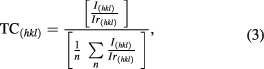
Figure 1(a) shows x-ray diffraction (XRD) spectrum of synthesized PbS nanosheets with space group Fm-3m (225). XRD spectrum was acquired using Cu-Kα x-rays of wavelength 1.5418 Å. All diffraction peaks in figure 1(a) were indexed to pure cubic phase of PbS (PDF card number 04-003-2980). No impurity peaks were observed in this spectrum. The lattice constant parameter (a = b = c) obtained from XRD spectrum is 5.940 640 Å. The volume of cell is 209.652 3358 Å3. The calculated cell volume and cell parameters agree well with the values given in the PDF card number 04-003-2980 (cell volume = 209.240 005 Å3 and a = b = c = 5.936 740 Å). From XRD spectrum texture coefficient ( ) can be calculated to visualize the different crystalline planes with degree of preferred orientation using the following relation [26]
where  specifies the intensity from PDF card (reference pattern),
  is the intensity taken from XRD spectrum of PbS nanosheets and integer n is the number of diffraction peaks under consideration. From this equation,
  for a randomly distributed powder material is less than 1 or equal to 1 for each crystallographic plane. However, it is greater than 1 for preferentially oriented planes [27]. Values of
  calculated for PbS nanosheets are listed in table 1. It can be seen that more preferably oriented plane with highest
  value (1.164) is (200).

Figure 1. (a) XRD spectrum and (b) EDS spectrum of synthesized PbS nanosheets. The inset to EDS spectrum shows TEM image of nanosheets.
Download figure:
Standard image High-resolution imageTable 1. X-ray diffraction intensities and preferred orientation factor for 2D cubic phase PbS nanosheets.
| PbS | |||||
|---|---|---|---|---|---|
| h | k | l | Ixrd | Icard | Texture coefficient |
| 1 | 1 | 1 | 85 771 | 913 | 1.116 501 |
| 2 | 0 | 0 | 97 856 | 999 | 1.164 156 |
| 2 | 2 | 0 | 56 150 | 679 | 0.982 809 |
| 3 | 1 | 1 | 33 924 | 396 | 1.018 125 |
| 2 | 2 | 2 | 17 073 | 217 | 0.935 06 |
| 4 | 0 | 0 | 9009 | 92 | 1.163 799 |
| 3 | 3 | 1 | 10 364 | 133 | 0.926 115 |
| 4 | 2 | 0 | 17 416 | 229 | 0.903 862 |
| 4 | 2 | 2 | 10 364 | 156 | 0.789 573 |
Energy dispersive x-ray spectroscopy (EDS) was used to find chemical composition of PbS nanosheets. The EDS spectrum is shown in figure 1(b). Occurrence of Pb and S peaks in this spectrum also endorse purity of prepared PbS nanosheets. Inset to the figure 1(b) is a low-resolution transmission electron microscope (TEM) image clearly showing existence of PbS nanosheets.
Figures 2(a) and (b) show a plot of real part of impedance (Z') and imaginary part of impedance (Z'') of PbS nanosheets from 210 K–300 K. Amplitude of the applied ac signal was 1 V and frequency of ac signal was 20 Hz–2 MHz. In these spectra frequency increases from right to left. Filled circles indicate experimental data whereas solid lines represent results fitted to experimental data using z-view software. At all temperatures two semicircular arcs can be seen clearly centered at high and low frequencies regions. Second semicircle can be seen more clearly as inset to figures 2(a) and (b) at higher frequencies. Semicircle at higher frequencies indicates bulk (grain effect) and semicircle at lower frequencies corresponds to grain boundary effect. The equivalent circuit used to fit the experimental data is shown in figure 2(c). Here Qg, Rg, Qgb, and Rgb represent constant phase element of grains, resistance of grains, constant phase element of grain boundaries and resistance of grain boundaries, respectively. Constant phase element is used to accommodate non-ideal capacitive behavior [28]. In this case [29] C = R(1−n)/nQ1/n, where n = 0 for pure resistor and n = 1 for pure capacitor. Figure 2(d) shows the variation of resistance and capacitance (calculated from fitting) of grains and grain boundaries of PbS nanosheets with temperature. We note that Rg is smaller than Rgb. Both Rg and Rgb decrease as temperature increase indicating thermally activated conduction at elevated temperatures. The value of Cgb increases and then decreases as temperature rises. The reason for this behavior is that initially, the more charge carriers are collected at grain boundaries due to existing defect states and hence capacitance increases. At higher temperature these defect states are removed. Conduction across the grain boundaries increases and hence Cgb decreases. On the other hand, Cg increases with an increase in temperature. This is because with increase in temperature more charge carriers are collected at grain interior due to the creation of ionic and electronic defects and hence Cg increases.
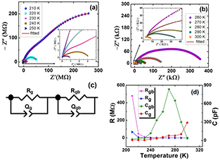
Figure 2. (a) and (b) electrical AC characteristics of PbS nanosheets at 210 K to 300 K from 20 Hz to 2 MHz (insets to Z' versus Z'' plots show second semicircle at higher frequencies), (c) equivalent circuits to model the system, and (d) the variation of resistance and capacitance of the grains and grain boundaries with temperature.
Download figure:
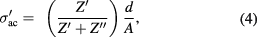
Standard image High-resolution imageFrequency and temperature dependent real part of complex ac conductivity  is determined using following equation [23]
where  and
and  is cross-sectional area and thickness of pellet respectively. Figure 3(a) shows
  versus frequency curve for PbS nanosheets. The values of
  for PbS nanosheets are much greater than those of PbS nanoparticles [30]. The
  is composed of two terms [31]

where  is the dc conductivity (low frequency region) caused by the drift of charge carriers and it obeys Arrhenius equation:

where  is Boltzmann's constant,
  is activation energy and
  is pre-exponential factor. For PbS nanosheets, Arrhenius plot is shown in figure 3(b) at 100 Hz. From this figure
  was found to be equal to 0.59 eV.
  depends on temperature as well as frequency and is given by [31]

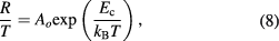
where B is a parameter and it has units of mho m−1. The s is also a parameter and it depends upon temperature. It has no units and is determined from slope of  . Figure 3(c) shows variation of s with temperature. Parameter s increases with increase in temperature indicating that possible conduction mechanism in PbS nanosheets is small polaron hopping process [32, 33] obeying following equation [34]
here  is pre-exponential factor and
  is activation energy associated with small polaron hopping process. Figure 4(a) shows
  versus
  curve for grains and grain boundaries of PbS nanosheets. The values of
  for grain boundaries and grains are found to be 0.54 eV and 0.52 eV, respectively.
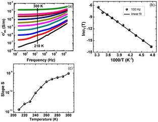
Figure 3. Electrical AC characteristics of PbS nanosheets at 210 K to 300 K from 20 Hz to 2 MHz: (a) variation of ac conductivity with frequency, (b) Arrhenius plot for activation energy calculation from linear fit, and (c) variation of slop s with temperature.
Download figure:
Standard image High-resolution image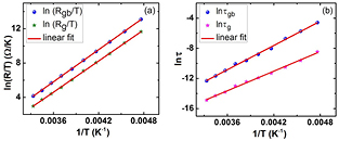
Figure 4. Electrical AC characteristics of PbS nanosheets at 210 K to 300 K from 20 Hz to 2 MHz: (a) variation of resistance of grain boundaries and grains with inverse of temperature, and (b) variation of relaxation time  of carriers at grain boundaries and grains with inverse of temperature.
Download figure:
Standard image High-resolution imageThe activation energy ( ) associated with relaxation time is defined as:

here τ = RC is time constant,  is pre-exponential factor. Figure 4(b) shows the relaxation time behavior of PbS nanosheets with temperature. From figures 4(a) and (b), we can see that the resistances and relaxation times of grain boundaries and grains decrease with temperature indicating thermally activated conduction and relaxation processes. The calculated activation energies of grain boundaries and grains of relaxation process are 0.46 eV and 0.37 eV, respectively. Conduction and relaxation processes have different activation energies. This may be attributed to the fact that conduction mechanism involves binding and hopping energies along with disorder while relaxation process contains hopping energy of polarons alone [32, 35].
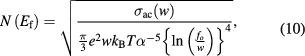
The density of states  of PbS nanosheets at Fermi level was calculated using ac conductivity values using the following relation [36]
where  is electronic charge,
  is localized wave function and
  is the photon frequency. The
  was determined by considering
  and
and  [37–39]. The
  of PbS nanosheets from 210 K–300 K at different frequencies is shown in figure 5(a). The
  of PbS nanosheets decreases with increase in frequency and it increases with increase in temperature and similar to the previous studies [37–39]. The
  values for PbS nanosheets are much higher than NiS2 nanoparticles reported earlier [40].
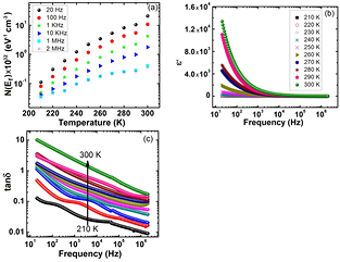
Figure 5. Electrical AC characteristics of PbS nanosheets at 210 K to 300 K from 20 Hz to 2 MHz: (a) variation of  with temperature, (b) variation of
  with frequency, and (c) frequency dependence of tan
 .
.
Download figure:
Standard image High-resolution imageFigure 5(b) shows real part of dielectric constant ( ) of PbS nanosheets at different frequencies and temperatures.
  has high values at lower frequencies and it decreases at higher frequencies. However, it is almost frequency independent above 104 Hz. The decline in dielectric constant is because polarization cannot align completely during a cycle of frequency in an available time. Such a situation occurs because different polarizations contribute to dielectric constant. At lower frequencies, net polarization appears due to combine effect of interfacial, electronic, atomic and ionic polarization [41–44]. When relaxation frequency is larger than the measuring frequency, each kind of polarization will create an impact on dielectric constant. Thus, at low frequency the interfacial polarization attributed to grain boundaries yielding the large quantity of dielectric constant. Maxwell–Wagner theory [45] of interfacial polarization best explains the dielectric constant variation with frequency. This theory is in a good agreement with Koop's phenomenological theory [46]. This theory tells that grain boundaries interfacial polarization due to trapped charges is prominent at lower frequencies because grain boundaries act as barrier to movement of charge carriers.
High values of  at low frequencies can be explained in two ways. First PbS nanosheets have high density of disordered ions with a specific surface such as positive ions of great number of lead gaps and negative ions of many sulfur vacancies acting as shallow accepters at grain boundaries [47]. The arrangement of these lead gaps and sulfur vacancies in PbS nanosheets may lead to creation of dipole moments. Applied electric field rotate many dipole moments. The rotation-direction polarization occurs at grain boundaries contributing to dielectric constant of PbS nanosheets. Second, at high pressure the interfaces or grain boundaries of compacted nanomaterials must contain an excessive deal of defects (dangling bounds, porosities, and vacancies). These defects at the grain boundaries cause the changing of negative and positive space-charge distributions [47]. On application of external electric field, the negative and positive space-charges at grain boundaries move towards positive and negative poles of electric field, respectively. In the meantime, a great number of dipole moments are created unavoidably after they have been trapped by defects [48]. Consequently, at grain boundaries the space-charge polarization results in a large dielectric constant for PbS nanosheets. Also, the huge increase in
  with temperature at lower frequencies is due to increase in interfacial polarizations by thermally activated dipoles, assembling at grain boundaries. In frequency independent region
  above 104 Hz. Similar trend has been detected in Bi2S3 nanorods [24] and NiS2 nanoparticles [40] where
  above 105 Hz and
  above 103 Hz, respectively. Also, high value of dielectric constant of PbS nanosheets as compared to PbS nanoparticles [30].
Variation of  (loss tangent) with frequency is shown in figure 5(c). In these spectra a maxima is observed at all temperatures that advocates existence of relaxing dipoles. With increase in temperature, the maxima in loss spectra shifts towards higher frequency signifying reduction of relaxation time and hence reduction of diffusion of ions [49]. A decrease in
  at higher frequency shows small number of electrically active defects [50]. PbS nanosheets have low dielectric loss as compared to PbS nanoparticles [30] and NiS2 nanoparticles [40]. These variable and high values of dielectric constant make the PbS nanosheets excellent material for important technological dielectric applications.
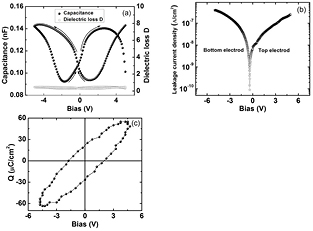
A major application of dielectric materials is in manufacturing of capacitors. PbS nanosheets capacitor has very low dielectric loss of 0.48–0.27 at ±5 V as calculated from figure 6(a). On application of sinusoidal signal of 1 MHz having amplitude 10 V (peak-to-peak) stable CV and QV hysteresis was observed. Figure 6(a) shows the capacitance and dielectric loss from −5 V to +5 V for PbS nanosheets capacitor. The stable butterfly loop was observed due to switching of ferroelectric polarization [51]. The permittivity calculated at 0 V capacitance was ~150 and the dielectric loss remained below 0.50. Further, increase in bias to ±20 V showed sharp rise in dielectric loss but the dielectric breakdown did not occur.
Figure 6. (a) Capacitance and dielectric loss factor of PbS nanosheets capacitor as a function of applied voltage, (b) capacitor dc leakage current of PbS nanosheets as a function of applied voltage, and (c) QV loop of a PbS nanosheet capacitor at 300 K and 1 MHz frequency.
Download figure:
Standard image High-resolution image
Measured dc leakage current densities are shown in the figure 6(b). We can see that current densities remain below 0.5 µA cm−2 in the range ±5 V. A 5 s delay time after each 0.1 V step was used. Sawyer–Tower QV hysteresis measurements were done with ±5 V peak voltage and 1 MHz frequency applied across the PbS pellet and QV loop is shown in the figure 6(c). A symmetric remnant polarization was observed such as ±Pr of 23 µC cm−2 (2Pr = 46 µC cm−2). The coercive voltage and field are 2 V and 0.02 kV cm−1, respectively. The remnant polarization (23 µC cm−2) with dielectric loss (<0.50) for PbS nanosheets is much higher than the remnant polarization (0.005 µC cm−2) with dielectric loss (~0.07) for NiS nanoplates reported earlier [52].
Here we compare our results with previously published results. The  for PbS nanosheets is 1.164 for 200 plane while
  for PbS thin films is 6.65 for 200 plane [53]. Electrical conductivity for PbS nanosheets is of the order of 10−3 S m−1 while for PbS thin films is 1.64 S m−1 [53]. The highest value of
  is 14 000 for PbS nanosheets while for PbS thin films the highest value of
  is 425 [54–56]. The
  for PbS nanosheets is ⩽10 while for PbS thin films is ⩽750 [54].
4. Conclusions
Two-dimensional PbS nanosheets were prepared using solid state reaction method. The purity and morphology of PbS nanosheets were characterized by XRD, TEM, and EDS. Z' versus Z'' plots clearly indicate presence of grain and grain boundary phases of PbS nanosheets from 20 Hz–2 MHz. The temperature was varied from 210 K–300 K. Resistance of grain and grain boundary decreases with increase in temperature obeying thermally activated conduction. Small polaron hopping mechanism was found to be conduction mechanism in PbS nanosheets. Conductivities in PbS nanosheets were relatively higher as compared to PbS nanoparticles. High value of dielectric constant of PbS nanosheets was obtained as compared to Bi2S3 nanorods and NiS2 nanoparticles. PbS nanosheets have high value of DOS of the order of 1032 eV−1 cm−3 as compared to NiS2 nanoparticles. The stable butterfly loop was observed due to switching of ferroelectric polarization in CV measurements. The permittivity at 0 V capacitance was ~150 and the dielectric loss remained below 0.50. The QV measurements showed a remnant polarization 23 µC cm−2 in PbS nanosheets.
Acknowledgments
M F Afsar would like to acknowledge the Higher Education Commission of Pakistan for the financial support through International Research Initiative Program (IRSIP). Authors are thankful to Dr T Y Yan of Nanyang Technological University Singapore for his help in TEM analysis. M A Rafiq would like to acknowledge Higher Education Commission for financial support under National Research Program for Universities (NRPU Project No 3662).