

Abstract
In the present work nanostructures of tin oxides were synthesized by a microwave-assisted thermal oxidation. Tin precursor powder was loaded into a cylindrical quartz tube and further radiated in a microwave oven. The as-synthesized products were characterized by scanning electron microscope, transmission electron microscope, and x-ray diffractometer. The results showed that two different morphologies of SnO2 microwires (MWs) and nanoparticles (NPs) were obtained in one minute of microwave radiation under atmospheric ambient. A few tens of the SnO2 MWs with the length of 10–50 µm were found. Some parts of the MWs were decorated with the SnO2 NPs. However, most of the products were SnO2 NPs with the diameter ranging from 30–200 nm. Preparation under loosely closed system lead to mixed phase SnO–SnO2 NPs with diameter of 30–200 nm. The single-phase of SnO2 could be obtained by mixing the Sn precursor powders with CuO2. The products were mostly found to be SnO2 nanowires (NWs) and MWs. The diameter of SnO2 NWs was less than 50 nm. The SnO2 NPs, MWs, and NWs were in the cassiterite rutile structure phase. The SnO NPs was in the tetragonal structure phase. The growth direction of the SnO2 NWs was observed in (1 1 0) and (2 2 1) direction. The ethanol sensor performance of these tin oxide nanostructures showed that the SnO–SnO2 NPs exhibited extremely high sensitivity.
Export citation and abstract BibTeX RIS

Original content from this work may be used under the terms of the Creative Commons Attribution 3.0 licence. Any further distribution of this work must maintain attribution to the author(s) and the title of the work, journal citation and DOI.
1. Introduction
Nanomaterials have been explored to bring new technologies which have a prodigious impact to the scientific and industrial revolution [1, 2]. This is because their novel properties lead to a wide range of applications. The semiconductor oxides are also the promising nanomaterials for nanotechnology. Hence, synthesis processes of these nanostructures are investigated intensively to control shape, morphology, and size, and to optimize cost-power consumption balance.
Among the semiconductor oxide nanomaterials, SnO2 is one of the good candidates for various applications such as solar cells [3], gas sensors [4], light emitting diodes [5], photocatalyts [6], and lithium-ion batteries [7]. This is due to their good thermal and chemical stability, low electrical resistivity and high light transmittance. Many techniques for synthesis of tin oxide nanostructures have been reported such as hydrothermal route [8], thermal evaporation [9], and thermal oxidation [10]. The assistance of microwave radiation has already seen in hydrothermal route and thermal evaporation technique, which provide a good product quality, saving time and power consumption [7, 11]. However, there are only a few reports on thermal oxidation technique [12, 13].
In this work tin oxide nanostructures including SnO2 nanoparticles (NPs), SnO–SnO2 NPs, and SnO2 nanowires (NWs) were synthesized rapidly by a simple thermal oxidation technique in atmospheric ambient with assistance of microwave radiation. The formation of tin oxide nanostructures was discussed. The obtained SnO and SnO2 nanostructures were used in ethanol sensors. Their ethanol sensor performances were characterized and compared.
2. Experimental
2.1. Synthesis of tin oxide nanostructures
Tin oxide nanostructures were simply synthesized from Sn powder by microwave-assisted thermal oxidation (MWTO) technique whose details can be found elsewhere [12, 13]. First, 2.0 g of Sn powder was loaded into a cylindrical quartz tube with diameter of 2.8 cm and length of 10 cm in a household microwave oven (SHARP), as shown in figure 1. Note that one end of the tube was closed. The Sn powder was radiated by microwave power of 700 W at a frequency of 2.45 GHz under atmospheric ambient. During the microwave radiation, occurrence of spark could be seen inside the tube. The Sn powder was heated for only one cycle of microwave process and holding times of 60 s. After cooling down the system, the quartz tube was taken out from the microwave oven. The white product and a few long wires were observed in the quartz tube. In the case when the both ends of the quartz tube were closed loosely, the soft-green product could be observed. By mixing 2.0 g of Sn powder with 0.4 g of CuO2 and one end closed, the white wool product could be seen at the Sn powder and on the both ends. Finally, these products were collected for characterizations of morphology and crystal structure by using scanning electron microscope (SEM), transmission electron microscope (TEM), and x-ray diffractometer (XRD).

Figure 1. Schematic illustration of the preparation system using the MWTO technique.
Download figure:
Standard image High-resolution image2.2. Ethanol sensing measurement
SnO2 NPs, SnO–SnO2 NPs, SnO2 NWs, and SnO2 microwires (MWs) were sonicated in ethanol and screened on fluorine doped tin oxide glass (FTO glass) with interdigitated electrodes to fabricate sensors. To characterize ethanol sensing, each sensor was connected to an electronic circuit and then exploded to 50 ppm of ethanol concentration for 150 s at operating temperature of 376 °C, 412 °C, 450 °C, 486 °C, and 524 °C. These irrational temperature points were the sensor temperatures which corresponded to controller set point of 420 °C, 460 °C, 500 °C, 540 °C, and 580 °C. Then the SnO–SnO2 NPs were further characterized with 100 ppm and 500 ppm of ethanol. It was carried out through a gas flow-through system with 1 ml min−1 air flow as a reference gas. The concentration of ethanol was generated from ethanol solution at 34 °C in the ethanol breath simulator (GUTH laboratory Inc., USA). The electrical resistance of the sensors was measured using a volt-amperometric technique. The sensitivity was defined as the electrical resistance in air to that in the explosion of gas,  .
.
3. Results and discussion
3.1. Synthesis and characterization
In the case of Sn powder with one end closed, the white product, which was later confirmed as SnO2 NPs, was mostly found on the wall of the quartz tube and at the center of the tube where the Sn precursor powder was placed. Figure 2(a) shows the typical SEM image of the SnO2 NPs, which reveals the particles size of 30–300 nm. Whereas, a few of SnO2 MWs with diameter of about 1 µm and length of about 10−50 µm were observed at the wall of the quartz tube. In the case of Sn powder with two closed ends, the soft-green product was exposed as only SnO NPs and SnO2 NPs (SnO–SnO2 NPs) which were mostly found at the ends of the quartz tube. Figure 2(b) shows the typical SEM image of the SnO–SnO2 NPs. It reveals feature as similar as the first case. In the case of mixing Sn powder with CuO2, the white wool product was exposed as SnO2 MWs and SnO2 NWs that were found on the Sn powder and at both ends of the quartz tube, respectively. Figures 3(a) and (b) show the morphology of the SnO2 MWs. It reveals that the surface of the SnO2 MWs is not smooth with diameter of about 1 µm, whereas, figures 3(c) and (d) show the tiny and curved wire of the SnO2 NWs with diameter of about 50 nm. The straight length of the NWs is in the range of 200–1000 nm. The NWs was connected together to create a special NW network. Whereas the SnO2 NWs obtained by the conventional thermal oxidation [10] was straight and their length was upto several ten micrometers. The short length of the SnO2 NWs in this work is possibly due to the high temperature difference between the vapor source (Sn powder) and the formation place (the ends of tube).
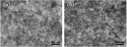
Figure 2. SEM images of (a) SnO2 NPs and (b) SnO–SnO2 NPs.
Download figure:
Standard image High-resolution image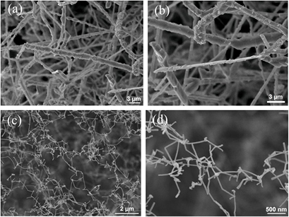
Figure 3. SEM images of (a) SnO2 MWs, (b) two-times magnification of (a), (c) SnO2 NWs, and (d) three-times magnification of (c).
Download figure:
Standard image High-resolution imageX-ray diffractometry analysis, as shown in figure 4, exposes that the white product and the white wool product are the cassiterite or tetragonal rutile SnO2 with lattice parameter of a = 4.738 Å and c = 3.187 Å (JCPDF 41-1445). In addition, the soft-green product composes of the cassiterite SnO2 and the tetragonal SnO with lattice parameter of a = 3.802 Å and c = 4.838 Å (JCPDF 72-1012). Moreover, no peak of any compounds of Cu was observed.

Figure 4. XRD profile of the tin oxide nanostructures.
Download figure:
Standard image High-resolution imageThe products were further characterized using TEM and selective area electron diffraction (SAED) for size and phase structure, respectively. Figure 5 shows a typical TEM bright field image of the tin oxide nanostructures. Figure 5(a) reveals the some part the SnO2 NPs with a clear surface of particles and diameter of 50–100 nm. The SAED in the inset also confirms their phase structure of the cassiterite SnO2. Figure 5(b) shows the TEM image of the SnO–SnO2 NPs. It reveals that some particles were covered with fine particles. This is possible that the fine particles might be the SnO NPs that covered on the SnO2 NPs. However, there was no evidence to confirm this aspect due to limit of the instrument. The analysis only confirmed that the SnO–SnO2 NPs compose of both phase, as seen in the inset of figure 5(b). Figure 5(c) shows TEM image of the SnO2 NWs. Most of the SnO2 NWs are short but link together to form a large NW network. Their size at the joint is bigger than middle wire which is less than 50 nm. Figures 5(d) and (e) show single NW with the inset of the corresponding SAED, indicating growth direction of (1 1 0) and (2 2 1), respectively.
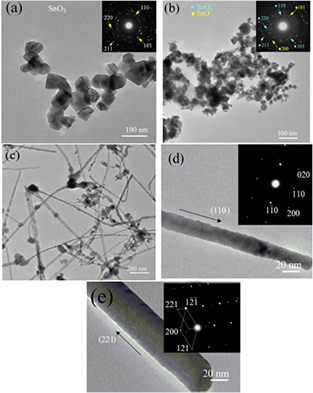
Figure 5. TEM images of (a) the SnO2 NPs, (b) the SnO–SnO2 NPs, (c) the SnO2 NWs, and (d)–(e) single NW with growth direction. The insets show the corresponding SAED.
Download figure:
Standard image High-resolution imageThe formation of the SnO2 nanostructures can be explained in the term of the supersaturation ratio, which affects to the nucleation probability [9] as given by
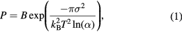
where B is a parameter constant, σ is the surface energy of the crystal plane, kB is the Boltzmann's constant, T is the absolute temperature, and α is the supersaturation ratio between the actual vapor pressure and the equilibrium vapor pressure corresponding to the temperature T. The high supersaturation ratio leads to the explicit growth direction that possesses minimal surface energy, which results in formation of NWs. Conversely, the low supersaturation ratio leads to no significant probability among the crystal planes to grow, resulting in formation of NPs. In MWTO, the vapor of tin oxide was generated by thermal evaporation and thermal oxidation of Sn powder, where the heat was given by the microwave power. As seen in the results above, most of the product was in particle form for the case the Sn powder without CuO2. This indicates that the vapor of the tin oxide would not high enough for formation of NWs and resulted in the formation of the SnO2 NPs and the SnO NPs. The existence of the SnO NPs in the product might be due to the lack of oxygen in the closed system, which can be explained using the S–O phase diagram [14]. In addition, the CuO2 added into the Sn powder might act as catalyst that can increase the generation of tin oxide vapor, leading to the ultrahigh supersaturation ratio which result in the formation of the SnO2 NWs in a specific direction. As seen in the result, the (1 1 0) growth direction was observed due to its lowest surface energy. Moreover, SnO2 NWs that formed at the Sn powder were in such condition for a long time, resulting in large crystal size or the formation of the SnO2 MWs.
3.2. Ethanol sensing performance
To compare gas sensing performances of four different nanostructures of tin oxides namely SnO2 NPs, SnO–SnO2 NPs, SnO2 NWs, and SnO2 MWs, the electrical resistance of the sensors in air and in 50 ppm of ethanol at various operating temperatures was measured. Their sensitivity was calculated and the results were shown in figure 6(a). It can be seen that the sensor obtained from the SnO–SnO2 NPs exhibited extremely high sensitivity compared to that of others. The highest sensitivity was about 94 which obtained at the operating temperature of 486 °C. Therefore, the optimal operating temperature these sensors could be in 450–520 °C. In contrast, the SnO2 NWs and MWs exhibited very low sensitivity to ethanol. The sensitivity versus the operating temperature of the SnO–SnO2 NPs for various ethanol concentration was shown figure 6(b). The highest sensitivity was 164 and 577 for 100 and 500 ppm of ethanol concentration, respectively, at the operating temperature of 486 °C. Furthermore, figure 6(c) shows the typical graph presenting the resistance change in explosion of ethanol gas against time for the SnO–SnO2 NPs at 486 °C. The log scale of the resistance was set to show the difference of Rgas in various ethanol concentration. The resistance drastically changed when ethanol gas was on but gradually recovered when ethanol gas was off. The recovery time was more than 20 min and increased as the ethanol concentration increased. This drawback is normal occurred when the sensitivity is high due to the lack of oxygen replacement. In addition, after ethanol testing, the color of the SnO–SnO2 NP film was still similar as before testing. This could be indicated the stability of the SnO–SnO2 NP film in ethanol sensing environment.

Figure 6. Plot of sensitivity against the operating temperature for (a) all tin oxide nanostructures samples with 50 ppm of ethanol; (b) the SnO–SnO2 NPs sample with 50, 100 and 500 ppm of ethanol and (c) plot of resistance against time in various ethanol concentration for the SnO–SnO2 NPs sample at 486 °C.
Download figure:
Standard image High-resolution image
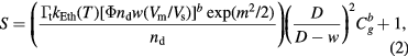
The sensitivity of semiconductor oxide such as ZnO, TiO2, or SnO2, can be explained by using the sensor response formula [15] as following
where  is time constant,
  is a reaction rate constant between adsorbed oxygen species and ethanol vapor depends on the operating temperature,
  is a ratio of surface area per volume of material (
 ),
),  is density of donor electron which is assumed to be constant,
  is depletion layer width,
  is the system volume,
  is an oxygen species parameter having value of 1 for
  and 0.5 for
  ,
,  is the reduced depletion depth, defined as
  ,
,  is Debye length,
  can be used as diameter of nanoparticle or nanowire, and
  is ethanol concentration. The better sensitivity of SnO–SnO2 NPs and SnO2 NPs over the SnO2 NWs and MWs can be explained in the term of surface to volume ratio in the formula, which that of the NPs is greater than that of the NWs and MWs. Nonetheless, the higher sensitivity of the SnO–SnO2 NPs over the SnO2 NPs could be explained in the term of the depletion width due to p-n junction formation at the interface between p-SnO and n-SnO2 NPs [16]. Therefore, SnO–SnO2 contact could create the larger depletion width over SnO2–SnO2 contact. This resulted in higher ethanol sensitivity of the SnO–SnO2 NPs compared to that of SnO2 NPs in this work and in previous reported [11, 17, 18]. In addition, the p-n junction led to much higher sensitivity to hydrogen gas of SnO/SnO2 nanoposites over that of SnO2 NPs [19].
4. Conclusion
The tin oxide nanostructures namely SnO2 NPs, SnO–SnO2 NPs, and SnO2 NWs, were simply synthesized in a short time using MWTO technique. The analysis indicated that the SnO2 NPs and NWs were the cassiterite SnO2 with diameter of 30–300 nm and less than 50 nm, respectively. The growth directions of SnO2 NWs in (1 1 0) and (2 2 1) were observed. The SnO NPs were the tetragonal SnO with diameter of 30–300 nm. The characterization of gas sensing showed that the SnO–SnO2 NPs exhibited the greater sensitivity over that of others
Acknowledgments
This research was partially supported by the Young Researcher Grant from Chiang Mai University.
Footnotes
- *
Invited talk at 5th Thailand International Nanotechnology Conference (Nano Thailand-2016), 27–29 November 2016, Nakhon Ratchasima, Thailand.