

Abstract
Array structures of CdS-sensitized ZnO nanorods (NRs) were fabricated on conducting substrates of indium tin oxide (ITO) that serve as working electrodes in photoelectrochemical (PEC) cells for the generation of hydrogen by splitting of water. The ZnO NRs were synthesized by the hydrothermal method at low temperature with different growth times; structures of CdS-sensitized ZnO NRs were created by the dipping method with various dipping times to optimize the efficiency of splitting water. It was found that maximum photoconversion efficiency of an electrode made from CdS-sensitized ZnO NRs with a growth time of 3 h and a dipping time of 30 min under simulated solar irradiation of 100 mW cm−2 was about 2.7%. The rate of evolution of H2 gas generated from the water-splitting process was also measured. A maximum rate of 22 ml cm−2 was achieved after 1 h exposure, which is higher than with CdS–ZnO NR electrodes in previous studies.
Export citation and abstract BibTeX RIS

Original content from this work may be used under the terms of the Creative Commons Attribution 3.0 licence. Any further distribution of this work must maintain attribution to the author(s) and the title of the work, journal citation and DOI.
1. Introduction
The utilization of metal oxides as photoelectrodes for harvesting light and splitting water in a photoelectrochemical (PEC) cell is a promising means of producing renewable energy. This is desired because the use of fossil fuels is responsible for climate change though the release of greenhouse gases [1, 2]. The first study of PEC splitting of water on TiO2 photoelectrode was reported by Fujishima and Honda in 1972 [3], and since then metal oxides such as ZnO, WO3 and α-Fe2O3 [4–6] have also been investigated for splitting water, with various morphologies and structures because of their appropriate band gap and flat band potential, low electrical resistance and good resistance to corrosion in aqueous solution [7]. One of these, ZnO, is being intensively investigated because it has a wide range of possible synthesis techniques and a highest electronic mobility that would be favorable for electron transport [8, 9].
A major obstacle in the use of metal oxides is the large band gaps and the lack of absorption in the visible region of the spectrum of sunlight. An additional issue for films with 0D nanoparticles is charge transport and photon absorption, which are often limited because of a lack of continuous conducting pathways and the loss of photons by reflection of light from the surface [10]. 1D nanostructures are expected to have improved charge-transport properties and reduced photon loss due to reduced reflection [11]. In order to efficiently absorb light it is necessary to sensitize the photoelectrode by various narrow band-gap materials such as CdS, CdSe, CdTe, CuInS2 etc [12, 13]. Among these sensitizing materials, CdS has been widely used because of its narrow direct band gap (2.4 eV) and a suitable band alignment with ZnO. The energy levels of its conduction and valence bands lie higher than those of ZnO, leading to easy electron injection from the conduction band of CdS to the conduction band of ZnO and movement of holes to the CdS–electrolyte interface. These processes can efficiently separate generated electron–hole pairs and thus suppress their recombination. However, to date no materials or nanostructures have been found to encompass all of these issues, and the apparent measurement of evolved hydrogen is still lacking.
In this report we present the combination of two advantages: (i) using a structure made from ZnO nanorods (NRs) as a scaffold to enhance charge-transport efficiency and (ii) an external CdS coating to form a structure of CdS/ZnO NRs, which is anticipated to enhance the efficiency of solar energy conversion in a PEC cell. The thickness of deposited CdS is controlled to optimize the efficiency by optimizing the optical–electrical properties of the structure. Besides the theoretical evaluation of the efficiency of splitting water, we also attempt to design an H2 gas collection system and consider the possibility of practical application of fabricated electrodes.
2. Experiment
2.1. Preparation of the ZnO NRs
Prior to the growth of the films of ZnO NRs, the Zn metal layer was deposited on a pre-treated indium tin oxide (ITO) substrate by DC sputtering for 1 min and then annealing at 500 °C for 2 h to serve as the seed layer. The arrays of ZnO NRs were formed on the seeded-ITO substrate by a hydrothermal method. In a typical synthesis, an aqueous solution of zinc nitrate [Zn(NO3)2.6H2O] and hexamethylenetetramine (C6H12N4) mixture (ratio 1:1) was prepared with a concentration of 0.04 M. The seeded-ITO substrates were placed in the solution and ZnO NRs were grown at 90 °C for various times (1, 2, 3, 4, 6 and 12 h). The obtained products were washed with deionized (DI) water then dried in a flow of dry nitrogen.
2.2. Preparation of the CdS/ZnO NRs
The structures of ZnO NRs grown for 3 h that exhibited the best efficiency were further decorated with CdS layers by the dipping method. The ZnO-NR/ITO electrodes were incubated in an aqueous solution of 10 mM Cd(NO3)2.4H2O and 10 mM C2H5NS at room temperature for 15, 30, 60 and 90 min then rinsed thoroughly with DI water and dried with N2 flow.
2.3. Characterization of the ZnO structures
The crystalline structures and morphologies of the ZnO NRs and CdS/ZnO NRs were examined by x-ray diffraction (XRD, Rigaku D/MAX-RC) using Cu-Kα radiation and by scanning electron microscopy (SEM, JEOL JSM-700F). A UV–vis spectrophotometer (S-3100, SCINCO Co.) was used to measure the optical absorption spectra.
2.4. Photoelectrochemical measurement
PEC properties were measured using a three-electrode electrochemical analyzer (potentiostat/galvanostat model 263A, USA); the ZnO and CdS/ZnO films were used as the working electrode, a Pt grid as the counter electrode and Hg2Cl2/Hg in saturated KCl as the reference electrode. An electrolyte of 0.01 M of Na2SO4 and a UV light source with wavelength of 365 nm and intensity of 0.3 mW cm−2 (Z169609-E-Series UV lamp) were used for the ZnO structures. An electrolyte of 1 M of Na2S and a visible light source (150 W Xe lamp with intensity of 100 mW cm−2 passing through an AM 1.5 G filter) were also employed to evaluate the efficiency of the CdS/ZnO electrodes. The potential was swept linearly at a scan rate of 10 mV s−1. The illuminated area of the working electrode was fixed at 0.25 cm2 using a nonconductive epoxy coating. The photoconversion efficiency is calculated from the equation
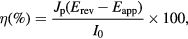
where Jp is the photocurrent density (mA cm−2), I0 is the power density of incident light, Erev is the standard state-reversible potential (which is 1.23 V (versus normal hydrogen electrode, NHE)), the applied potential is Eapp = Emeas − Eaoc, where Emeas is the electrode potential (versus standard calomel electrode, SCE) of the working electrode at which photocurrent was measured under illumination and Eaoc is the electrode potential (versus SCE) of the same working electrode under open-circuit conditions [14].
2.5. The measurement of evolved hydrogen
The evolved hydrogen was collected using a reverted burette. The experimental setup is shown in figure 1.

Figure 1. Experimental setup of hydrogen generation.
Download figure:
Standard image High-resolution image3. Results and discussion
The morphologies of the structures of ZnO NRs grown on the ITO substrate with various growth times of 1, 2, 3, 4, 6 and 12 h are depicted in figures 2(a)–(f), respectively. They show the change in density, diameter and length of NRs with growth time at a constant concentration of 0.04 M. With increasing growth time the diameter and length of NRs increased but their density NRs decreased because of coalescence and fast growth direction to c-axis direction of NRs [15].

Figure 2. Images of the morphology of structures of ZnO NRs with various growth times: (a) 1 h, (b) 2 h, (c) 3 h, (d) 4 h, (e) 6 h and (f) 12 h.
Download figure:
Standard image High-resolution imageFigure 3 shows SEM images of CdS/ZnO NRs obtained with different dipping times of 15, 30, 60 and 90 min. It shows that the CdS nanoparticles cover the entire surface of the ZnO NR from root to tip and the covering is fairly uniform. The thickness of the CdS layer increases for a longer dipping time. For a dipping time of 60 min, the clogging of NR–NR gaps begins, and it is seen more clearly for a dipping time of 90 min. This is a disadvantage for a PEC cell because the surface area in contact with the electrolyte decreases.

Figure 3. SEM images of structures of CdS/ZnO NRs with various dipping times: (a) 15 min, (b) 30 min, (c) 60 min and (d) 90 min.
Download figure:
Standard image High-resolution imageFigure 4(a) shows XRD patterns of structures of ZnO NRs and of CdS/ZnO NRs with rods grown for 3 h and a CdS dipping time of 30 min. The peaks (1 0 0), (0 0 2), (1 0 1), (1 0 2) and (1 1 0) are of the hexagonal phase of the wurtzite structure of ZnO. The peaks (1 1 1), (2 2 0) and (3 1 1) are of the cubic phase of CdS. This indicates that the sample is composed of CdS and ZnO, and the broadening of CdS peaks demonstrates that CdS grows on the surface of ZnO as nanosized particles. The size of the CdS particles coating the ZnO nanorods was 9 nm, as determined by the Scherrer formula [16].

Figure 4. (a) XRD patterns and (b) UV–vis spectra of ZnO NRs and CdS/ZnO NRs.
Download figure:
Standard image High-resolution imageFigure 4(b) shows UV–vis absorption spectra of ZnO NRs and CdS/ZnO NRs with a CdS dipping time of 30 min. The results show that the bare ZnO absorbs only in the UV region at wavelengths shorter than 400 nm, but with the CdS coating on the ZnO the absorption edge is extended to the visible light region at a wavelength of 550 nm. Therefore, ZnO sensitized by CdS nanoparticles would efficiently capture visible light.
Figure 5 presents photocurrent and dark-current densities and the corresponding UV photoconversion efficiencies for photoelectrodes made from ZnO NRs with different growth times (1, 2, 3, 4, 6 and 12 h). Figure 5(a) shows the influence of the growth time and the applied potential bias on the magnitude of the photocurrent. Under UV illumination, the anodic photocurrent increased with increasing potential bias and reached saturation at 1.2 V in the range of potential from −0.6 V to 1.2 V for all samples. Correspondingly, figure 5(b) is the photoconversion efficiency. It shows an increase when the growth time is increased and reaches a maximum of about 23% for a growth time of 3 h, then decreases as the growth time increases further. This result suggests that a large ratio of surface area to volume is a key factor for a high efficiency of NRs, which is in good agreement with observation of the SEM image (figure 3). As the reaction time increases, the diameter and length of NRs increase, but their density becomes sparser. We thus believe that the maximum efficiency observed for a reaction time of 3 h is due to the highest ratios of surface area to volume and efficient diffusive transport of photogenerated holes to oxidizable species in the electrolyte, ultimately minimizing recombination losses.

Figure 5. (a) Photocurrent and dark-current densities and (b) corresponding UV photoconversion efficiencies of ZnO NRs with various growth times.
Download figure:
Standard image High-resolution imageFigure 6 shows the photocurrent density and solar photoconversion efficiency of electrodes made from CdS/ZnO NRs with various dipping times. The results show that the photoconversion efficiency increased with the dipping time to a maximum of 2.7% for a CdS dipping time of 30 min. The efficiency decreased when the CdS dipping time increased further. This can be explained as follows: with increasing thickness of the CdS layer the light absorption increases, leading to a greater number of electron–hole carriers. However, when the thickness exceeds its optimal value, the light absorption is not efficient, and the CdS layer acts as a potential barrier for charge transfer. Therefore, the recombination or trapping of electron–hole pairs was higher, causing the decrease in efficiency [17].

Figure 6. (a) Photocurrent and dark-current densities and (b) corresponding solar photoconversion efficiencies of CdS/ZnO NRs with various dipping times.
Download figure:
Standard image High-resolution imageThe rate of evolution of H2 gas generated from the water-splitting process was measured for the samples of CdS/ZnO NRs for a dipping time of 30 min and for pure ZnO NRs for comparison as shown in figure 7. The result shows that the rate of H2 generation increased linearly with increasing exposure time. The sample CdS/ZnO NRs with a dipping time of 30 min achieved a volume of 22 ml cm−2 after 1 h exposure, which is higher than with electrodes made from pure ZnO NRs and CdS/ZnO NRs in other studies [18].

Figure 7. Volume of H2 gas generation under illumination with sunlight.
Download figure:
Standard image High-resolution image
4. Conclusion
We fabricated structures of CdS/ZnO NRs for use as photoanodes in a PEC cell for hydrogen generation. The photoconversion efficiency was optimized by controlled time-dependent growth. ZnO NRs showed a maximum efficiency of 23% for a growth time of 3 h under UV light illumination; CdS/ZnO NRs showed maximum efficiency of 2.7% for a dipping time of 30 min under solar illumination, and the volume of H2 gas generated was 22 ml cm−2 after 1 h exposure. The results show that the photoanodes made using a structure of CdS/ZnO NRs is promising for application in energy-to-hydrogen conversion devices.
Acknowledgment
This work is supported in part by the Grant-in-Aid for Scientific Research code B2016-DQN-04, 2016–2017 from the Ministry of Education and Training, Vietnam.