

Abstract
Two-dimensional (2D) arrays of gold nanodisks (Au NDs) with different sizes of 75, 95 and 115 nm, with the distances between NDs of 10, 30 and 50 nm were fabricated on square-inch substrates. The optimal conditions regarding the thickness of anodic aluminum oxide (AAO) template, sputtering time and annealing temperature for Au, lift-off the walls of AAO template for getting the highest quality 2D arrays of Au NDs have been determined. Morphology and surface plasmon resonance (SPR) absorption of the 2D arrays of Au NDs were examined by using appropriate techniques. The 2D arrays of fabricated Au NDs show different SPRs peaking in the spectral range of 600–1600 nm, which are very promising for surface-enhanced Raman scattering (SERS)-based sensor applications. As an example for the potential use of fabricated SERS substrates, we have demonstrated the detection of methamidophos at various concentrations ranging from 1 ppb to 103 ppm. Moreover, the method we have used to fabricate the 2D arrays of Au NDs can be applied to other kinds of metals or alloys just by varying the targets in the sputtering process.
Export citation and abstract BibTeX RIS

Original content from this work may be used under the terms of the Creative Commons Attribution 3.0 licence. Any further distribution of this work must maintain attribution to the author(s) and the title of the work, journal citation and DOI.
1. Introduction
Raman scattering spectrum is a fingerprint for a certain molecule, a molecular group, glassy or crystalline matters because it shows specifically the vibrational modes or optical phonons of the checked sample. The use of Raman scattering spectroscopy is therefore a very direct manner to detect molecular groups or different structural phases [1–5]. However, in conventional Raman scattering spectroscopy the light scattering signal is typically weak due to small cross sections of 10–30–10−29 cm2 per molecule in most cases. The surface enhanced Raman scattering (SERS) effect was discovered during the seventies of the last century [2, 6]. There are two mechanisms, which have been commonly accepted to explain the enhancement effect. One is based on the electromagnetic excitation of localized surface plasmons, and the other is based on the formation of charge-transfer complexes at the surface of metallic nanostructures. For most cases, SERS enhancement occurs due to surface plasmon resonance (SPR) of metallic nanostructures. Since the discovery of the SERS effect, there have been a number of works done mainly concerning realization of new substrates to have localized surface plasmons resonant at the suitable spectral ranges, and concerning the techniques to detect single molecule [7–9]. The localized surface plasmon resonances (LSPRs) induce huge enhancement of electromagnetic fields as 'hot spots' where the specimens experience a giant excitation and scattering with the enhancement factor proportional to the fourth power of the ratio of the enhanced electric field to the incident excitation field [10]. In attempt to realize the high sensitive detection of different molecules, pathogens, etc just by directly taking Raman scattering spectra from normal vibrations specific to specimens, the LSPRs from various kinds of nanostructured metals have been performed and widely studied [2, 5, 7–11]. As claimed in the literature, LSPRs can enhance the Raman scattering up to 14 orders of magnitude compared to that without LSPRs [10, 12], that is due to electrical field enhancement at the surface of nanostructured metals. Comparing to fluorescence, if one can enhance the Raman scattering of 14 orders of magnitude, the Raman scattering signal can be 3 orders of magnitude larger than that from fluorescence spectroscopy. This is because the small Raman scattering cross sections are compensated, while the shorter vibrational relaxation times in Raman scattering compared to the much longer electronic transition times in fluorescence result in the number of Raman photons being much larger than fluorescence photons emitted per the same unit time. In practical Raman scattering measurement, it needs the enhancement factor of 108 in order to be able to detect the signal from a single molecule.
Among nanostructured metals, whose optical characteristics are supported by LSPRs, Au and Ag nanoparticles (NPs) have been widely studied and showed giant enhancement in Raman scattering [5, 7–12], fluorescence [13], and photovoltaics [14]. For profiting from SERS effect, one can: (i) directly use the hot electromagnetic field on the surface of metallic NPs which are randomly distributed in colloidal form or adsorbed on the surface of other nanostructures, substrates [15–17]; or (ii) use the very hot electromagnetic field formed in between nanostructured metals, such as in two-dimension (2D) arrays of metallic nanostructures [10, 12, 16, 17]. Recently, Nguyen et al [11] has presented a review on main SERS substrates which have been fabricated until now. For each kind of metal, depending on the size and shape of nanostructured metals and dielectricity of their environment around, the plasmon resonance wavelength is peaking differently. When these nanostructured metals are arranged in close proximity to each other, they interact together to red-shift the resonance wavelength [18–20].
There has been a number of publications devoted to the SPR of metallic NPs or disks prepared by different methods [2, 5, 7, 18]. Most of them presented the systems with larger particles and small distance between the particles (in a few nm), or small particles with large distance between them. Practically, both diameter and distance are very important to contribute to the plasmonic resonance from which one may have appropriate applications. Using chemical methods, we have successfully made 2D arrays of the 50 nm Au NPs [18]; and those of Ag NPs with different sizes of 20–50 nm [21]. However, it is difficult to prepare larger Au/Ag NPs with narrow size distribution and good spherical shape, and very difficult to arrange them separately to be stable at the distance of tens of nanometers. Another difficulty in arranging Au/Ag NPs into 2D arrays by chemical method is that the surface coverage is usually not very high due to the low dispersion stability of surface-functionalized Au/Ag NPs [18, 21]. Using physical methods, like the nano-lithograph patterning technique, that enables the high spatial resolution, accuracy, reproducibility and periodic arrangement of the nanostructures. However, these physical methods are almost impractical to produce large SERS substrates because they require expensive equipments and the production is normally very low (as an example, we have ever fabricated a periodic 2D array of 150 nm gold on Si wafer by nanolithography; it took 5 h to obtain a small-area of 20 × 20 μm2). There have been other methods to have SERS substrates by using templates for further filling of Au. For preparing 2D templates, one can arrange polystyrene nanospheres on certain solid substrates [22]; or using nanoimprint lithography [23]. An effective approach could be the application of anodic aluminum oxide (AAO) membranes as masking template to obtain the ordered 2D arrays [24–28]. We do expect that by using a combined method of sputtering Au onto the AAO templates, the large square-inch 2D arrays of Au nanodisks would be fabricated for SERS applications.
In this paper, we present the success in development of an efficient method to fabricate 2D arrays of Au NDs by sputtering Au to fill in AAO template, then lifting-off the walls of template. The optimal conditions regarding the thickness of AAO template, sputtering time and annealing temperature for Au, lifting-off the AAO template, have been determined to fabricate square-inch 2D arrays of Au NDs. The 2D arrays of Au NDs were fabricated with different mono-sized Au NDs of the 75, 95 and 115 nm diameters; and with different distances between NDs of 10, 30, and 50 nm. The fabricated 2D arrays of Au NDs show different SPRs peaking in the spectral range of 600–1600 nm, which are very promising for the potential use in SERS, because of many excitation laser available in this spectral range. As an example of using fabricated 2D arrays of Au NDs, we demonstrated the detection of methamidophos (MAP) at different concentrations ranging from 1 ppb to 103 ppm.
2. Experimental
2.1. Preparation of AAO templates
AAO templates with the pore diameters (D) ranging from 35 to 115 nm and the pore wall thickness (d) from 0 nm (i.e., AAO is fully being etched) to 90 nm were prepared following a method described in the literature [28]. In brief, we prepared the AAO templates by a two-step anodization process. For preparation, high purity aluminium foil (5 N) was cut into 4 × 4 cm2 pieces and cleaned in acetone, alcohol and deionized water. Then, these aluminium foil pieces were electro-polished in a mixture of alcohol and perchloric acid (4:1 volume ratio) at 7 °C and 20 V for 2 min to get the mirror-like surface aluminium foils. The first anodization was performed in a 0.3 M oxalic acid solution at 10 °C for 90 min under variously applied voltages (from 20 to 50 V) depending on the desired interpore distance. The anodically formed aluminum oxides were completely stripped by immerging into a mixed solution of H3PO4 and CrO3 (3:1 volume ratio) at 65 °C for 30 min. The resulting imprints were used as the templates for further processing. The second anodization on the resulting imprints was done in the same conditions as those of the first anodization for 1 min to make the AAO membrane of 100 nm thick. The pores were then widened in the diluted 0.1 M H3PO4 aqueous solution at 30 °C. The pore sizes and the thicknesses of the walls between the pores were controlled by etching time for several tens of minutes. We did the experimental correlation between the D and d of AAO templates as a function of etching time; then go further with the AAO templates that have the desired D and d. For all cases, we kept the second anodization for 1 min to make the AAO membrane of 100 nm thick.
2.2. Fabricate of 2D-arrays of Au NDs
2D-arrays of Au NDs were fabricated by filling Au into the nanopores of AAO templates, then annealing, and finally removal of AAO templates. Au was filled into the nanopores of the AAO template by magnetron sputtering technique at the RF power of 20 W, under 0.6 Pa pressure of argon, for 15 min. After that, the Au-filled AAO template was annealed at 450 °C for 30 min in open atmosphere to solidify Au on Al2O3. This heat treatment was done to really improve the quality of the Au NDs. Finally, the walls of the AAO template were removed in 0.5 M H3PO4 aqueous solution for 30 min.
2.3. Morphological, structural and optical characterizations
Morphologies of the fabricated 2D-arrays of Au NDs were visualized from the scanning electron microscope (SEM) images (using a S-4800 FE-SEM Hitachi equipment). The absorption spectra from SPR of Au NDs 2D-arrays were recorded using an UV–vis-NIR double-beam spectrometer (Varian Cary 5000). To test the SERS effect of the fabricated 2D-arrays of Au NDs as SERS substrates, we did measure the Raman scattering spectra of MAP, which is an organophosphorus insecticide and acaricide widely used to control a variety of horticultural and agricultural pests. The Raman scattering spectra were taken using a Raman spectrometer (Jobin Yvon, model LabRam-1B) or just a lab set-up system which is composed of a Nd:YAG laser (Teem Photonics, 1064 nm, 2 mW at the sample) as the excitation source, a 55 cm focal length spectrometer (iHR550 Horiba) equipped with a 2-stage Peltier-cooled CCD (Synapse Horiba).
3. Results and discussion
Figure 1 shows the experimental calibration for the pores diameter D of AAO templates as a function of etching time. With increasing the etching time, D is widened causing d is thinned. These calibration curves are very helpful to guide for further preparation of AAO templates having various D and d. Note that the first anodization is very important to determine the interpore distances, consequently the final D and d values of AAO templates. In the first anodization, the applied voltage plays a crucial role to vary the desired interpore distances. For the interpore distances desired, we have applied the voltages over the range from 20 to 50 V to cover D from 40 to 115 nm. After determining all the relevant parameters necessary for further experiments, we intentionally prepared the two series of AAO templates having: (i) different D of 75, 95, and 115 nm, while d was kept to be the same of 10 nm for all kinds of Ds; and (ii) the same D of 75 nm but the d values were variously controlled to be of 10, 30, and 50 nm. For both series, the voltages applied in the first anodization were 34, 42 and 50 V to have the right interpore distances. Then, for series (i), it took 50, 65 and 80 min to get the pores diameters of 75 nm, 95 nm and 115 nm, respectively; and for series (ii), it took 50 min, the same etching time, to get the same D of 75 nm, while d remained in between the pores would be of 10, 30, and 50 nm.

Figure 1. Pores diameter (D) of AAO templates as the function of etching time.
Download figure:
Standard image High-resolution imageFigure 2 shows typically the SEM images of the two mentioned series of AAO templates. One can see very nice AAO templates with different D and d as designed, that are expected to be the appropriate preparation for fabricating 2D arrays of Au NDs which have the SPR covering the spectral range of lasers available for the excitation in Raman spectroscopy (e.g., lasers emitted at 785, 980, 1064, 1350, 1500 nm).
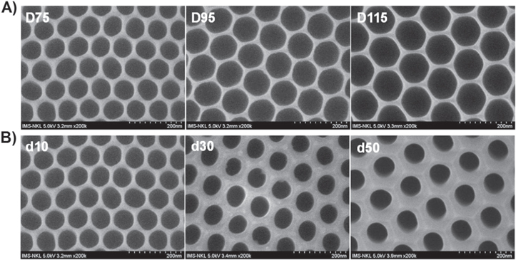
Figure 2. SEM images of the AAO templates with (A) the same 10 nm separation between the pores (d, the pore wall thickness) while the pore diameters D are 75, 95, and 115 nm; and (B) the same 75 nm D with separations between the pores d are 10 nm, 30 nm, and 50 nm as indicated in the images, respectively.
Download figure:
Standard image High-resolution imageThe two series of AAO templates presented in figure 2 were used to prepare the two series of 2D arrays of Au NDs with D and d following the AAO templates. Figure 3 shows the SEM images of the resultant 2D arrays after sputtering to fill Au into the nanopores of the AAO templates, annealing and lifting-off the AAO walls. These two series of the 2D arrays of Au NDs have been fabricated to serve for the separate study on the red-shift of the SPR with size/diameter of Au NDs; and the blue-shift of the SPR with increasing the distance between Au NDs. The thickness of the sputtered Au layer was controlled by sputtering time. The same technical procedure as before, the thickness calibration was done to determine the duration times for sputtering that enable to produce Au layers with thicknesses corresponding to the required ones. Based on the calibration data, we have determined the sputtering time of 15 min for fully filling Au into the nanopores of AAO templates to obtain the suitable and good quality Au coating for further processing. The Au-filled AAO templates were annealed at 450 °C for 30 min in open atmosphere to make Au more rigid on Al2O3 and easier lifting-off process for removal of the top-part of AAO templates, while remaining Au NDs. The sizes of the Au NDs and their separations can be estimated from the magnified parts of the SEM images, showing that they follow closely to those from the AAO templates. In the present case, large area (square-inch) AAO templates have been made by chemical method, and then 2D arrays of Au NDs were fabricated following inexpensive and efficient method. These fabricated 2D arrays of high density Au NDs that formed 'hot-spots' between Au NDs to induce the great enhancement of the electromagnetic field, consequently making SERS activity very efficient.

Figure 3. SEM images of 2D arrays of Au NDs prepared by sputtering Au onto the AAO templates (correspondingly presented in figure 2) and then lifting-off the walls of AAO templates.
Download figure:
Standard image High-resolution imageThe 2D arrays of Au NDs having larger D would have the SPR at longer wavelengths; the red-shift of the SPR with size/diameter of Au NDs; then controlling d to vary the peaking resonance wavelengths. At smaller d, interaction between Au NDs is stronger to shift more the plasmon resonance to the longer wavelength side. In the literature, one can see the two resonances at shorter wavelength which almost no change with size and the one at longer wavelength which have red-shift with bigger sizes of Au nanodisks [29]. Our observation is consistent with calculation results reported in the literature. One should note that for the SPR appeared in the literature, most are from bigger or smaller sized Au NDs, or from more distant Au NDs. In our case, we have presented the plasmon resonances from Au NDs in rather moderate sizes and separate at different distances. Positively, the plasmon resonances are achieved in the wavelengths coincident with lasers which are commonly used as the excitation sources in Raman spectroscopy. Figure 4 shows the SPR characteristics of the fabricated 2D arrays with (A) the same 10 nm separation between the pores while the pore diameters are (a) 75, (b) 95, and (c) 115 nm; and (B) the same 75 nm pore diameter but the separations between the pores are 10, 30, and 50 nm. One can see clearly from the first series of Au NDs arrays that with increasing diameter of Au NDs the SPR shifts to the longer wavelength side. The SPRs peaking at 1300, 1450, and 1600 nm were observed for the 75 nm, 95 nm, and 115 nm Au NDs, respectively (figure 4(A)). For the 2D arrays fabricated from the same 75 nm Au NDs arranging with the separations between NDs of 10, 30, and 50 nm, we observed the SPRs peaking around 600 nm, 850 nm, and 1300 nm, respectively (figure 4(B)). There is a clear tendency that the closer Au NDs interact stronger consequently making more red-shift of the SPR. In our previous paper, we have showed that the colloidal 50 nm Au NPs have the plasmon resonance at around 540 nm, while putting them into a 2D array with the separation between NPs of several nanometers the plasmon resonance was red-shifted to around 670 nm [18]. We have also tried to have the regular AAO templates to arrange Au NDs into the regular arrays with the period comparable to the wavelength of the incident light to expect that the light–particle interaction causing the diffraction waves. However, it is not the case because our fabricated 2D arrays are not perfectly regular. These fabricated 2D arrays of high density Au NDs that formed 'hot-spots' between Au NDs to induce the great enhancement of the electromagnetic field, consequently making SERS activity very efficient.
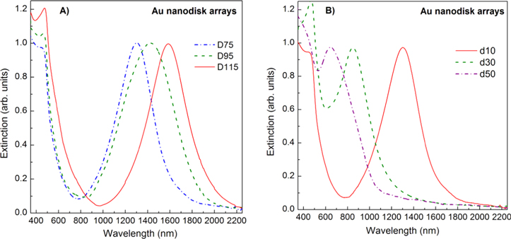
Figure 4. Plasmon resonances from 2D arrays of Au NDs in (A) the same 10 nm separation between the NDs while the diameters of Au NDs are 75, 95, and 115 nm; and (B) the same 75 nm diameter Au NDs with the separations between them are 10 nm, 30 nm, and 50 nm as indicated in the figures, respectively.
Download figure:
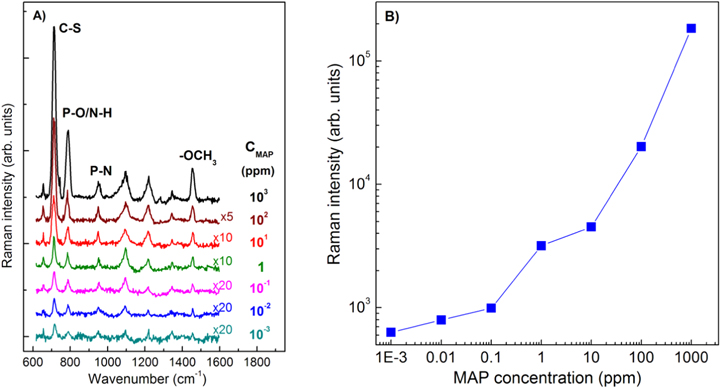
Standard image High-resolution imageTo check the possibility of using the fabricated SERS substrates, we have performed Raman scattering measurement for different samples such as glucose, virus H5N1, pesticides, etc. Among the samples, MAP is a highly efficient organophosphorus pesticide, which has the molecular formula as C2H8NO2PS. Figure 5(A) shows typically the Raman spectra of MAP loaded on a 2D array of the 75 nm diameter, 10 nm separation Au NDs, under the excitation by the 1064 nm laser light. MAP was loaded with various concentrations ranging from 1 ppb to 103 ppm. The choice of 1064 nm laser excitation light is for resonance with the surface plasmon of the fabricated Au NDs 2D array. Also, under the excitation by infrared light, one can avoid the interference from fluorescence. The Raman scattering spectra show the Raman peaks originating directly from the normal vibrations of molecular groups from MAP [30]. We have marked some Raman modes in the figure and taken the intensity of the 700 cm−1 Raman line, which is resulting from the C–S vibrational mode, to determine the concentration of MAP (figure 5(B)). For a concentration of MAP of 1 ppb we could still observe clearly the corresponding Raman scattering. Note that without the SERS effect one cannot take any Raman scattering spectrum of such a low MAP concentration of ppb. The results have shown the potential application of Au NDs 2D arrays as SERS substrates. The detailed and systematic study to determine the enhancement factor for Raman scattering of the fabricated 2D arrays of Au NDs is in progress. The results demonstrate that the fabricated SERS substrates are very promising for detection of a variety of pesticides, herbicides and diseases pathogens. One more point we would like to emphasize is that the 2D array fabricated by our procedure are really very stable, even after cleaning by ultrasonic for enough time to have multiple use.
Figure 5. (A) Raman scattering spectra of MAP at different concentrations loading on the 2D array of Au NDs with the 75 nm diameter and 10 nm separation; (B) the Raman intensity of the C–S vibrational mode (at ∼700 cm−1) as a function of the MAP concentration.
Download figure:
Standard image High-resolution image
4. Conclusion
In conclusion we have developed an efficient method to fabricate 2D arrays of Au NDs by sputtering Au onto AAO template, then lifting-off the walls of template. We have determined the optimal conditions regarding the thickness of the AAO template, sputtering time and annealing temperature for Au/AAO that are 100 nm, 15 min and 450 °C respectively to fabricate the highest quality 2D arrays of Au NDs. The two series of square-inch 2D arrays of Au NDs were systematically fabricated and studied: (i) with different diameters of 75, 95, and 115 nm, while the separation between NDs was kept to be the same of 10 nm; and (ii) with the same NDs diameter of 75 nm but the separations between NDs of 10, 30, and 50 nm. The fabricated 2D arrays of the Au NDs showed different SPRs peaking in the spectral range of 600–1600 nm, which are very promising for SERS-based sensor applications. As an example for the potential use of fabricated SERS substrates, we have demonstrated the detection of MAP at different concentrations ranging from 1 ppb to 103 ppm. We have observed clearly a tendency that the plasmon resonance shifts to the longer wavelength with increasing the size of Au NDs and with decreasing the distance between them. In addition, the method we have used to fabricate the 2D arrays of Au NDs can be applied to other kinds of metals or alloys just by varying the targets in the sputtering. Because of the attraction of Raman spectroscopy itself as a fingerprint technique, and additional SERS to enhance very much the Raman signal, Raman spectroscopy with SERS could become as a fast, direct, sensitive and unique technique to detect biomolecules, pesticides, herbicides etc.
Acknowledgments
This work was supported by Ministry of Science and Technology of Vietnam (e-ASIA project 33/2013/HĐ-NĐT). We thank the National Key Laboratory for Electronic Materials and Devices (VAST/IMS) for the use of facilities.