

Abstract
Water soluble nearly monodisperse CdSe nanocrystals have been successfully synthesized via aqueous phase solvothermal route in non ionic surfactant glycolic acid ethoxylate 4-non phenyl ether (GAEPE). X-ray diffraction (XRD), field emission scanning electron microscopy (FESEM) and transmission electron microscopy (TEM) are used to determine the phase, structural parameters such as lattice constants, strain, x-ray density and specific surface area, morphology, shape and size distribution, respectively, whereas optical properties are studied by UV-visible absorption and photoluminescence (PL) spectroscopy. All the diffraction peaks of XRD pattern indexed to wurtzite phase of hexagonal system of CdSe and crystallite sizes estimated to be 13–29 nm along some stronger and narrower peaks which is also consistent with TEM measurement while crystallinity and defects have been analyzed with selective area electron diffraction (SAED) pattern. Optical absorption spectrum shows that the as prepared sample exhibits primary and secondary absorption band centered at 2.15 eV and 1.82 eV, respectively, which is blue shifted as compared to bulk value (1.74 eV) of band gap due to quantum confinement effect. Photoluminescence spectrum shows sharp excitonic emission band centered at 583 nm which is nearer to primary band gap energy.
Export citation and abstract BibTeX RIS

Original content from this work may be used under the terms of the Creative Commons Attribution 3.0 licence. Any further distribution of this work must maintain attribution to the author(s) and the title of the work, journal citation and DOI.
1. Introduction
Semiconductor nanocrystals have attracted extensive research attention due to their size and shape dependent unique optical and electronic properties derived from the quantum confinement effect of both electrons and holes in all three dimensions, leading to an increase in the effective energy band gaps of the nanocrystals [1–4]. The properties of semiconductor nanocrystal (NC) changed drastically when the bulk size materials are scaled down to nanoscale. Therefore it is essential to understand how they influence the particle size, shape and size distribution on structural and optical behavior [5, 6]. Among the reported semiconductor nanocrystals, CdSe having a bulk band gap of 1.74 eV has been considered to be a most promising II–VI semiconductor material because of the possibility of wide tuning of its optical band gap to cover the whole visible range by varying the particle size [7–9]. Tailoring of this exotic semiconductor, make it promising for potential applications in the field of photonic ranging from biology (biolabeling/bioimaging) [10–13], energy (photovoltaics) [14–16] and light emitting devices [17–20].
Several stabilizing agents such as various surfactants, organic or inorganic polymers, thiols, amines and polyphosphates have been reported in the literature for the synthesis of NCs [21–25]. They have long chain organic molecules acts as a capping agent would give rise to a barrier to aggregation and hence passivate the particles. Typically, trioctylphosphine oxide (TOPO) [21], thiols [22], and dendron [23–25] have been used in surface modification and passivation of semiconductor NCs. High quality monodisperse synthesis of CdSe NCs has been reported by pyrolysis of organometallic cadmium reagent with organic coordinating solvents for over one and half decades [26, 5]. These are expensive, toxic, hazardous and insoluble in aqueous solution, hence, not compatible with biological system. It is of interest to modify the surface of semiconductor NCs with functional organic groups. This may be achieved by glycolic acid ethoxylate 4-non-phenyl ether (GAEPE), which is typically used to cap the particles during synthesis, with functional molecules. GAEPE, which is known as anionic surfactant is generally used for the pharmaceutical purpose and it is non-toxic, cheaper compared to other organic coordinating solvents. Surfactants are usually organic compounds that are amphiphilic, which contain both hydrophobic groups and hydrophilic groups. Therefore they are soluble in both organic solvents and water. The main reason to choose GAEPE as a surfactant because of their ability to form micelle in aqueous solution that helps in tailoring the CdSe nanocrystals such as sub-spherical, spherical, whisker and spindle whisker shaped nanostructures.
In the present investigation, water soluble CdSe NCs was synthesized by simple procedure including the use of less-expensive, less toxic and more environmentally benign reagents and solvents via eco-friendly solvothermal approach. In this approach, we report a convenient and controllable synthetic method based on a complex reaction in an aqueous system, which can produce nearly monodisperse CdSe NCs at low temperature 180 °C. Na2SeO3, Cd(NO3)2, and the reductant hydrazine hydrate are used as reactants in this method. One of the more significant advantages over pyrolysis method is that there is no need to inert atmosphere during the reaction process on contrary to requirement of inert atmosphere in pyrolysis of organometallic cadmium reagent at an elevated temperature. Because of simple reaction apparatus and low reaction temperature and time duration, this novel method will have a good prospect in future large-scale synthesis of water soluble CdSe NCs. Although, the quality of nanocrystals resulting from low-temperature aqueous based solvothermal synthetic method is not as good as that obtained under inert atmosphere at an elevated temperature organic-based methods.
Up to now, to best of our knowledge there is no report on successfully synthesis of water soluble CdSe NCs in GAEPE via aqueous phase solvothermal approach in ambient atmosphere. In this communication, we report the preparation of nearly monodisperse CdSe nanocrystals using non-ionic surfactant GAEPE and their structural and optical properties are investigated.
2. Experimental section
2.1. Materials
All the chemicals are used without further purification. Cadmium acetate bihydrated (CH3COO)2Cd.2H2O, molecular weight (mw) 268.52; anhydrous sodium selenite Na2SeO3, mw 173.01; hydrazine hydrate N2H4H2O, mw 50.06 were purchased from LOBA Chemie and glycolic acid ethoxylate 4-non phenyl ether (C19H34O6), average Mn ∼ 600, in liquid from supplied by Sigma-Aldrich, which was used as nonionic surfactant.
2.2. Synthesis of CdSe in glycolic acid ethoxylate 4-non phenyl ether matrix
A separate solution was made by dissolving 0.2595 g sodium selenite in 10 ml hydrazine hydrate and it was named as solution I. Another one separate solution was prepared by dissolving 0.1850 g cadmium acetate into the 10 ml double distilled water with constant stirring for 15 min. Further, 5 ml GAEPE was mixed into the resulting solution and then added 25 ml double distilled water. The whole mixture was constantly stirred for an hour and named as solution II. Solution I was slowly mixed into solution II with constant stirring for an hour, resulting solution turned into orange color. The final solution was transferred into teflon tube at 180 °C for 6 h and allowed to cool at room temperature and aged for 24 h. Thereafter solution is washed with ethanol and warm double distilled water several times through centrifuge. The color of obtained precipitate was brownish-black, which was ultrasonicated and kept into hot air oven at 60 °C for overnight. The powder was collected after dried the sample.
2.3. Characterization of sample and instrumentation
Structural information such as crystallite size, phase, x-ray density, strain and specific surface area for the nanocrystals was determined by XRD on a Rigaku miniflex-II operating at 30 KV, 15 mA using Cu Kα radiation (1.540 56 Å) with Ni filter. The 2θ range used was from 20° to 80° in steps of 0.02° with a count time of 1 s. The shape, size, particle size distribution, stacking fault and miss orientations of CdSe nanocrystals were analyzed with transmission electron microscopy and selective area electron diffraction pattern using a TEM (model number FEI Tecni G2F30STWIN). Sample was prepared by suspending CdSe nanocrystals in water followed by sonication for 15 min in an ultrasonic bath. The specimen was prepared by depositing few drops of a prepared dilute solution. The copper grid was then air-dried under ambient conditions before analysis. Optical absorption spectrum of CdSe sample was recorded on a Perkin Elmer lambda 35 double beam spectrophotometer. Photoluminescence spectrum was recorded using Ar+ laser (power 25 mW) with 514.5 nm wavelength. This wavelength was used for the excitation of as prepared CdSe nanocrystals. For recording the luminescence spectrum, aqueous solution of CdSe nanocrystals was prepared by dispersing the CdSe nanocrystals powder in double distilled water with ultrasonication. The prepared solution was placed in quartz cubet and kept in sample holder. The laser light was adjusted in such a way so that the light could fall vertically downward into the sample in cubet. The fluorescence light was collected using optical fiber which was attached to the sample holder horizontally; the fluorescence emission was collected to 90° with incident laser light. Finally, the fluorescence light emission was detected using CCD (charge couple device) attached monochromator (Acton SP 2500, Princeton Instruments).
3. Results and discussion
3.1. XRD study
Figure 1 shows the XRD pattern of as synthesized CdSe nanocrystals. All the diffraction peaks in the XRD pattern of as prepared product can be well indexed to those of the pure phase of wurtzite CdSe (JCPDS card No.08-459) except only one peak at 2θ = 29.6° might be due to impurities of Se was detected and can be indexed to hexagonal phase of Se (JCPDS-73-0465). In addition, it is noticeable that the intensity of (100) and (101) peaks is digressive and that of (002) diffraction peak strengthens. Thus the XRD pattern can be indicative of the anisotropic shapes of CdSe sample. The Scherer's equation  [27], where k denotes the Scherrer constant, λ is the wavelength of the x-ray, β is the full width at half maximum (FWHM) and θ is the diffraction angle, is used to estimate the particle size from the width of some intense x-ray peaks. These values are presented in table 1. Hence it can be clearly seen from the table for CdSe nanocrystals, there is large variation in crystallite size corresponds to each individual reflection plane may be anisotropic growth of sample which is also consistent with those of the size measurement by size distribution TEM histogram (latter shown in figure 5).
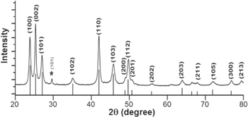
Figure 1. XRD pattern of as prepared CdSe nanocrystals synthesized by solvothermal route at 180 °C for 6 h.
Download figure:
Standard image High-resolution imageTable 1. Particles size calculated from some more intense peaks of XRD pattern for CdSe sample.
| CdSe sample | ||||||
|---|---|---|---|---|---|---|
| Plane | (100) | (002) | (101) | (110) | (103) | (112) |
| Particle size (nm) | 24.3 | 28.3 | 21.0 | 20.7 | 13.6 | 21.7 |
The strain value as well as effective particle size (i.e. the particle size with zero strain) is calculated somewhat directly by Williamson- Hall plot using formula [28]

where η represents strain whereas all the notations in this equation have usual meanings as already mentioned earlier. The graph is plotted between  as on y-axis and
  on x-axis as shown in figure 2. The intercept on y-axis gives effective grain size 23 nm while slope of graph provides strain value 0.78%.

Figure 2. Williamson-Hall plot corresponding to XRD pattern (figure 1).
Download figure:
Standard image High-resolution imageIt is known that for hexagonal structure the lattice parameter can be calculated by the following formula

where h, k and l are all integers, (hkl) is the lattice plane index and 'a' and 'c' are lattice constants. The strongest peak (002) is used to estimate the value of lattice constant 'c'. Calculated value of lattice constant is 7.019 Å which is slightly larger than the standard value 7.010 Å implying that the lattice expansion along c-axis and its value is found to be 0.13%. The lattice constant 'a', on the other hand, calculated 4.297 Å which is slightly lesser than the standard value 4.299 Å implying that the lattice contraction in this direction having value 0.07%. It is obvious that when one of the lattice parameters 'c' expand along c-axis, other lattice constant 'a' will be contracted and vice versa for hexagonal wurtzite system. Shahi et al [29] reported that for very small size of nanoparticles (2–5 nm), surface to volume ratio increases hence most of the atoms reside on their surfaces. Thus lattice of nanoparticles is distorted; it will become contracted or expanded.
Furthermore, x-ray density is calculated using following formula:  where ρ is the density (g cm−3), ΣA is the sum of the atomic weights of all the atoms in the unit cell, N is Avogadro's number and V is the volume of the unit cell (cm3). ΣA = nM, where n is the number of atoms per unit cell and M is the molecular weight. Inserting this value in above equation, therefore it takes the following form [30]

For wurtzite structure of CdSe, the number of atoms per unit cell is considered two therefore the calculated value of x-ray density, ρ = 5.662 × 10⁴ g cm−3. Moreover, the specific surface area of CdSe nanocrystals along the strongest plane is calculated using following formula [30]

where D and ρ are crystallite size and x-ray density of hexagonal CdSe nanocrystals, respectively. The value of specific surface area is estimate to be 3.78 × 105 cm2 g−1. Compared with standard value (JCPDS card No.08-459), the surface area increases, Maurya et al [31] reported that as the surface area increases surface energy will also be increased hence a higher number of active surface sites are produced. However increment in surface area is slightly greater than the standard value.
3.2. SEM study
Figure 3 show FESEM images of as prepared CdSe sample at different magnification. Figure 3(a) clearly shows the cauliflower shaped morphology having size less than 1 μm (nearly uniform with their size around 0.4 μm). Cauliflower like structure can be clearly seen at higher magnification as shown in figure 3(b). The SEM image therefore reveals that the CdSe NCs get assembled in GAEPE. The different sizes of cauliflower shaped structure have been shown by ovals in the SEM image (figure 3(b)).
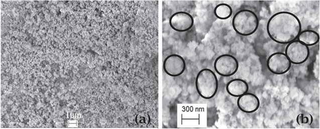
Figure 3. FESEM images of as synthesized CdSe sample.
Download figure:
Standard image High-resolution image3.3. TEM study
Transmission electron microscopy (TEM) was employed to examine the morphology, shape and size distribution of the as prepared CdSe sample. TEM images of solvothermally synthesized CdSe nanocrystals with corresponding selective area electron diffraction (SAED) pattern are shown in the figure 4. The prepared sample exhibits diverse morphology of as synthesized CdSe nanocrystals which is clearly shown in TEM images (figures 4(a) and (b)). It can also be seen, besides CdSe quantum dots, nanowiskers shaped structure also exhibit having mean length ∼18 nm and diameter at middle portion is ∼5 nm. TEM images of as prepared sample also display rather monodisperse CdSe nanocrystals having broad size distribution 3–29 nm.
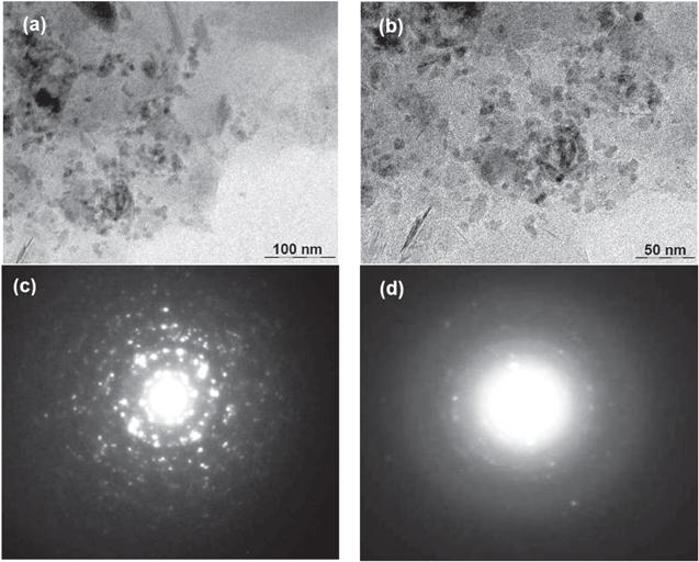
Figure 4. (a)–(b) TEM images of as prepared product and (c)–(d) their corresponding selective area electron diffraction patterns.
Download figure:
Standard image High-resolution imageThe SAED pattern of CdSe nanocrystals is very complicated (figures 4(c) and (d)). The SAED pattern (figure 4(d)) corresponding to figure 4(b) exhibits diffuse rings with few low intense spots revealing that small CdSe NCs has been layered by GAEPE. Thus the SAED pattern signifies the as synthesized CdSe NCs is polycrystalline in nature. The SEAD pattern (figure 4(c)) on the other hand, presents diffraction spot patterns corresponding to randomly oriented crystallites of CdSe reveal intense spotty patterns. Each diffraction spot has been elongated little at randomly and two or more spots either attach or overlap with each other, indicating that there are some small miss orientations, stacking faults and twin regions among the attached nanocrystal and also present texture. Texture in SAED pattern, is characterized by arcs of greater intensity in diffraction rings, which can be seen also in our case. Generally, larger crystals have spotty pattern.
The size distribution histogram corresponding to TEM images is shown in the figure 5. The particle size distribution histogram was plotted by calculating the size of about 100 CdSe nanocrystals using TEM micrographs. Size distributions are considered by taking the longest distance between the extreme points for each single nanocrystals of CdSe.

Figure 5. Particle size distribution histogram corresponding to TEM images (figures 4(a) and (b)).
Download figure:
Standard image High-resolution imageThe average size and size distribution (11 and 15 nm) for as prepared CdSe sample seems to be not closely belong to the size measurements for some more intense planes from XRD pattern. Since size determination by XRD corresponding to some more intense planes has value in 20–29 nm except only one plane which has the value 13.6 nm. It is believed that anisotropic growth of CdSe in GAEPE that gives the diverse morphology of CdSe such as sub spherical, elongated shape, whisker and spindle whisker shaped CdSe NCs. Hence the TEM histogram shows the broad size distribution with nanocrystals sizes in 3–29 nm and a significant amount of nanocrystals (nearly 60%) have sizes 7.5 nm ± 2.5 nm. However, a smaller amount of nanocrystals size distribution, nearly 15% nanocrystals, relative to whole size distribution lie in 17.5–27.5 nm (±2.5 nm) which is closer to sizes range (13–29 nm) determined by the XRD pattern. We have calculated the particle sizes for more intense and narrower peaks and not for comparatively lower intense and more broadened peaks. Since Stronger and narrower peaks of XRD correspond to the larger size which is evident from the TEM image as whisker shaped CdSe NPs having its length lies in 22.5–27.5 (±2.5 nm). Thus, the result derived from XRD pattern is in accordance with TEM observation.
3.4. UV-visible absorption spectroscopy
The absorption spectrum at room temperature for as synthesized CdSe sample is shown in the figure 6. Two shoulder peaks labeled at 568 and 689 nm having a long tail in which former is assigned as primary band gap whereas latter is assigned as secondary band gap as shown in figure 6(a). The pioneer of work for optical properties of CdSe NCs have been done by Morgan et al [32] and they have reported in degeneracy of valance band of CdSe NCs i.e. different states in valance band of CdSe have same energy. The primary band gap can be assigned to transition from the 1S light hole level to the lowest 1S electron level (h1SL–e1S) while the secondary absorption peak towards longer wavelength can be assigned to 1S heavy-hole level to lowest electron sub-band level (h1SH–e1S).
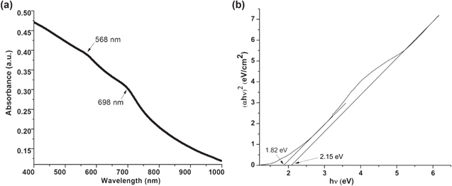
Figure 6. (a) UV-visible absorption spectroscopy of solvothermally synthesized CdSe sample and (b) corresponding Tauc plot.
Download figure:
Standard image High-resolution imageFurthermore, the optical band gap energy is calculated from the absorption spectra using Tauc equation

where hv is the photon energy, α is the absorption coefficient, Eg is the optical band gap energy, A is a constant and n = 1/2 for the direct band gap transition. In order to obtain the band gap for as synthesized CdSe samples, the curve (figure 6(b)) is plotted between (αhν)2 and hν. The extrapolations of straight lines to the ((αhν)2 = 0 give the values of band gap. The estimated values of optical band gap energy for sample are found to be 2.15 and 1.82 eV. The observed values of optical band gap is greater than the band gap of bulk CdSe (Eg = 1.74 eV) which is blue shifted due to quantum size effects in CdSe NCs. Utilizing the estimated value of band gap from the Tauc plot, the average particle size to be assumed spherical, can be determined using effective mass approximation (EMA) model of Brus which is given by equation as follows [1]

Here, Eg(nano) is the energy band gap of a nanocrystals, Eg(bulk) is the energy band gap of a bulk semiconductor,  and
and  are effective masses of the conduction band electrons and valence band holes of CdSe, respectively. The
  value for CdSe is reported as 0.11m0 [33], 0.13m0 [35] and
  value as 0.44m0 [35] and 0.63m0 [34], m0 being electron rest mass, ε is the dielectric constant of material having value 8.76 for CdSe, and ε0 is the space dielectric constant. The second term in above equation has very small contribution in the shift in band gap energy due to quantum size effect; hence it can be neglected. Thus the particle sizes of as synthesized CdSe samples are computed for light and heavy effective masses of conduction band electrons and valance band holes and their values are summarized in a table 2. As can be seen from the table 2, particle size estimated from the effective mass approximation (EMA) approximation model shows discrepancy with those of the size measurement with TEM suggesting weak quantum confinement effects because of irregular and anisotropic growth of CdSe nanocrystals having size larger than the 10 nm which is evident from TEM images as earlier. Since this model is effective for the small spherical shaped crystallite size of the order ∼10 nm.
Table 2. Particles size estimated using Tauc plot for CdSe sample by EMA approximation model.
| Band gap (eV) | Particle size (nm) estimated from EMA | |
|---|---|---|
for 
|
for 
|
|
| Epg = 2.12 | 6.62 | 6.00 |
| Esg = 1.83 | 13.80 | 12.57 |
 and
and  are effective mass of light hole and heavy hole, respectively, Epg is primary band gap, Esg is secondary band gap.
3.5. Photoluminescence study
Figure 7 displays the photoluminescence spectrum of as prepared CdSe nanocrystals with the excitation wavelength 514.5 nm. The emission profile is sharp and it can be seen that the emission energy (2.12 eV) is lower than the energy of primary band gap (2.15 eV). As the emission energy is not equal to the band gap, their difference gives the exciton binding energy (Ex) which depends on the material, is expressed by following relation [36]: Ex = Eg–hv. Inserting the value of Eg and hv, the value of Ex is obtained as 30 meV. The observed sharp peak centered at 583 nm is assigned to excitonic emission with binding energy 30 meV. Therefore we can conclude that the optical properties of CdSe nanocrystals also be controlled by exciton with exciton binding energy. Similar result has been reported by Sharma et al [36] and Chen et al [37]. They demonstrated that the formation of these nanocrystals relies on stabilizing interactions with the surfactant host.

Figure 7. Photoluminescence spectrum of as prepared CdSe sample with excitation wavelength 514.5 nm.
Download figure:
Standard image High-resolution image
4. Conclusions
Water soluble CdSe nanocrystals have been successfully synthesized in non ionic surfactant GAEPE by solvothermal route. XRD pattern exhibits the wurzite phase of hexagonal system with crystallite size of length 13–29 nm. Structural parameters such as lattice constants, strain, x-ray density and specific surface area have also been calculated. FESEM exhibits the as prepared product cauliflower shaped morphology. TEM images reveal as prepared CdSe NCs have diverse morphology such as sub-spherical, spherical, spindle whisker, whisker shaped nanostructures of length 3–29 nm. The average crystallite size and size distribution has been estimated to be 10 and 15 nm using size distribution histogram. The discrepancy occurs in size measurement with XRD to that of the TEM image due to diverse morphology (nanostructures) of CdSe. The absorption spectrum exhibits two shoulder peaks labeled at 568 and 689 nm having a long tail in which former is assigned as primary band gap whereas latter is assigned as secondary band gap. The primary band gap can be assigned to transition from the 1S light hole level to the lowest 1S electron level (h1SL–e1S) while the secondary absorption peak towards longer wavelength corresponds to secondary band gap assigned to 1S heavy-hole level to lowest electron sub-band level (h1SH–e1S). The optical band gap energy of both absorption bands is blue shifted compared to that of the band gap of bulk CdSe due to quantum confinement effect. Photoluminescence spectrum reveals the CdSe NCs shows sharp excitonic emission peak centered at 583 nm with exciton binding energy 30 meV. This novel method (aqueous phase solvothermal approach) will have a good prospect in future large-scale synthesis of water soluble CdSe NCs and their potential application in field of biological labeling/imaging, photo catalytic activities, photovoltaic and light emitting devices.
Acknowledgments
Authors are thankfully acknowledge to Prof. O N Srivastava Institute of Science, Banaras Hindu University (BHU), India for providing TEM facility and Physics Department, IIT BHU, India for XRD facility. One of the authors (A K Shahi) would like to acknowledge Centre of Excellence in Nanoelectronics (CENS), IISc Bangalore, India, for FESEM image through INUP user's program assisted by Mr Vardraj Premul and researcher Mr Prem Prakash Singh. AKS also gratefully to acknowledge CSIR, New Delhi, for providing senior research fellowship (SRF) award (Grant No.- 09/001/0359/2012/EMR-I) to carry out this work.