

Abstract
We describe the fabrication of highly sensitive graphene-based field effect transistor (FET) enzymatic biosensor for trace-detection of atrazine. The few-layers graphene films were prepared on polycrystalline copper foils by atmospheric pressure chemical vapor deposition method using an argon/hydrogen/methane mixture. The characteristics of graphene films were investigated by scanning electron microscopy, transmission electron microscopy and Raman spectroscopy. The results indicated low uniformity of graphene layers, which is probably induced by heterogeneous distribution of graphene nucleation sites on the Cu surface. The pesticide detection is accomplished through the measurement of the drain-source current variations of the FET sensor upon the urea enzymatic hydrolysis reaction. The obtained biosensor is able to detect atrazine with a sensitivity of 56 μA/logCATZ in range between 2 × 10⁻⁴ and 20 ppb and has a limit of detection as low as 0.05 ppt. The elaboration of such highly sensitive biosensors will provide better biosensing performances for the detection of biochemical targets.
Export citation and abstract BibTeX RIS

Original content from this work may be used under the terms of the Creative Commons Attribution 3.0 licence. Any further distribution of this work must maintain attribution to the author(s) and the title of the work, journal citation and DOI.
1. Introduction
In the last two decades, graphene has attracted much attention in many fields such as optoelectronics [1–3], composites [4], catalysis [5, 6], energy [7, 8], and sensors [8–13]. In particular, graphene has been regarded as a promising candidate for the development of highly sensitive biosensing systems thanks to its high charge mobility (∼105 cm2 V−1 s−1), large carrier capacity (∼1012 cm−2) and significant interface interactions with chemical/biological elements [14]. Since its introduction in 2004 [15], various graphene forms including single/bi/few-layered films, nanoribbons, exfoliated graphite nanoplatelets, reduced graphene oxide (rGO) composites etc, were incorporated into various types of sensors to improve sensing performances. For example, He et al [16] reported the label-free detection of the hormonal catecholamine molecules using liquid-gated field effect transistor (LgFET) based on parallel rGO arrays. The graphene flakes-based FET or electrochemical sensors were used to measure biomedical indexes (i.e., glucose) [17], monitor food safety (i.e., lactose) [18] and discriminate odorants (i.e., amyl butylrate) [19]. The limit of detection (LOD) of such sensors might be down to femtomole (fM) scale [17, 19]. Nevertheless, it still remains a great challenge to obtain reliable graphene sensing devices for high-throughput chemical and biological analysis in practical applications [20].
In this contribution we demonstrate the elaboration of a graphene LgFET urea enzymatic sensor for highly sensitive detection of atrazine. The graphene thin films prepared by atmospheric pressure chemical vapor deposition (APCVD) has been transferred onto the surface of source (S) and drain (D) electrodes. The use of CVD-grown graphene films in FET device will probably provide a promising approach for detection of targeted biomolecules.
2. Experimental
2.1. Synthesis of graphene films
Graphene films were grown by APCVD method on polycrystalline Cu foils (1.0 cm × 1.0 cm × 35 μm). First, the Cu foil was annealed at 1000 °C for 30 min in Ar (1000 standard cubic centimeter/minute (sccm))/H2 (300 sccm) gas mixture to reduce the native Cu oxide and to facilitate Cu grain growth. Then, a flow of methane (CH4, 30 sccm) was introduced to grow the graphene films. After 30 min, the CH4 flow was turned off and the Cu foil was rapidly cooled to room temperature under a flow of Ar (1000 sccm). Finally, the obtained Cu substrates covered by the graphene films were stored in ambient conditions. These graphene layers can be subsequently transferred onto any desired surfaces by wet-etching method right before use.
2.2. Characterization of graphene films
The scanning electron microscopy (SEM) images of the samples were obtained by using Hitachi S-4800. The graphene layer structure was studied using a high resolution transmission electron microscope (HRTEM, Fei Tecnai G20). Raman spectra were recorded using an Acton spectrometer fitted with a Pylon CCD detector and a 600 grooves/mm grating (∼2.5 cm−1 between each CCD pixel). The samples were characterized on Cu and using a 457 nm laser. The full width at half-maximum (FWHM) of the focused laser spot was about 400 nm.
2.3. Fabrication of the graphene based-FET sensor (GFET sensor)
The liquid gated FET sensor consisted of 19 coupled interdigitated electrodes, each of them has a source (S) and a drain (D), fixed on silicon substrate with 100 nm of thermal oxide (SiO2/Si) and one platinum wire top gate electrode (figure 1(b)). The S and D electrodes were fabricated on the SiO2/Si substrate by standard microfabrication techniques. The SiO2/Si wafer was spin-coated with a layer of photoresist and the shape of the electrodes was defined by UV-photolithography. Then, 20 nm of chromium and 200 nm of platinum were sputtered on top of the wafer and followed by lift-off. The configuration of designed electrodes was 60 × 60 × 2400 μm3 (width × gap × length). The source and drain measurement pads were protected from solution by covering the sample with silicone rubber (0.9 mm in radius) (figure 1(a)). The synthesized graphene films were released from the Cu substrate by wet-etching of the underlying Cu in 0.5 M iron chloride (FeCl3) solution for 10 min and then in 0.3 M ammonium persulfate (NH4)2S2O8 solution for 3 h. Following the etching, samples were rinsed with deionized (DI) water and then transferred onto the FET electrodes. The area of graphene film must be sufficiently large (∼1.8 × 1.8 mm2) to cover all 19 coupled interdigitated electrodes (figure 1(a)). Usually FET devices are fabricated by depositing metallic electrodes on top of the graphene films [21, 22]. Here, the graphene films have been directly deposited on top the prefabricated electrodes.

Figure 1. Schematic illustration of a FET device configuration (a) and the experimental setup (b) and (c) for electrolyte-gate GFETs.
Download figure:
Standard image High-resolution image2.4. Enzyme immobilization
The urease enzyme (EC 3.5.1.5, Merck) was diluted in phosphate-buffered saline solution and stored at 4 °C. This enzyme was immobilized on GFET sensors by cross-linkage via glutaraldehyde (GA) vapor (Sigma-Aldrich) for 1 h. To facilitate the immobilization of biomolecules, the graphene films (on FET device) were previously functionalized with carboxyl groups using an acidic mixture of HNO3:H2SO4 at volume ratio of 3:1. The electric pads were protected from GA molecules using a parafilm.
2.5. Atrazine detection
The detection of atrazine is accomplished through measuring changes in drain–source current of the FET sensor upon the urea enzymatic hydrolysis reaction. The urea solution (30 mM) and atrazine solutions (with concentrations ranging from 2 × 10⁻⁴ to 20 ppb) were prepared in deionized water. For each measurement, the FET sensor was incubated in the pesticide solution (positive sample) for 30 min and then characterized in urea solution. The variations of the drain–source current as a function of the gate voltage have been recorded to evaluate the inhibition of atrazine toward the enzymatic activity of urease. The electrical measurements of graphene LgFETs were carried out using a semiconductor parameter analyzer (Keithley, Model 4200-SCS). A control test was also conducted using a blank solution as a negative sample.
3. Results and discussions
3.1. Structural characterizations and morphology of graphene films
Figure 2 shows a typical SEM image of a graphene/few-layers graphene (graphene/FLG) film grown on Cu substrate at 1000 °C under flow of CH4 and H2 (CH4/H2 = 30/300 sccm) with a CVD duration of 30 min. As shown on figure 2, the entire surface of the Cu substrate is completely covered with graphene after 30 min growth. It was well established that the growth of graphene films is initiated by formation of nucleation sites on the substrate, followed by the planar spread of carbon atoms from those centers to form graphene domains, and finally finished by linking graphene domains to create a solid and stable graphene film [23]. Depending on reaction time, concentration of carbon source, substrate roughness, substrate area etc, the continuity of graphene films might be extended to several centimeters square [23]. The white lines observed on graphene film (figure 2) are graphene wrinkles. The appearance of the wrinkles is due to accommodation of the differences in the thermal expansion coefficients between graphene or graphite and Cu substrate [24].
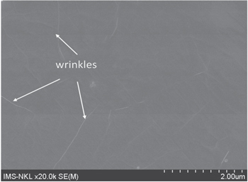
Figure 2. SEM image of graphene/FLG films grown on the Cu substrate after CVD process for 30 min.
Download figure:
Standard image High-resolution imageOn figure 3(A) an optical microscopy image of a graphene/FLG film after the CVD process of 30 min is presented. Figure 3(B) presents Raman spectra measured on the graphene/FLG covered Cu substrate measured at seven different locations (labelled from a to g on figure 3(A)). As expected, the two characteristic peaks assigned to G band (∼1580 cm−1) and 2D band (2730 cm−1) of graphene/FLG material were easily detected at all measured points. The defect related peak (D band) located around 1370 cm−1 is also present on some spectra (a, b, f and g). As inferred from the intensity ratio between G and D bands, the structural quality of the graphene/FLG film is rather good. At points e and f, additional features related to copper oxide [25] are also observed. From the analysis of Raman data, we can conclude (this was also confirmed by Raman mapping, not shown) that (i) the graphene/FLG film is covering the entire surface and (ii) the number of layers is varying from place to place as shown, for example, by the variation of G band integrated intensity from one spectrum to another (only the spectra where the copper oxide is not detected should be considered here since Raman intensities can be modulated depending on the oxide thickness [25]). Deducing the exact number of layers from the Raman spectra requires however more experiments and analysis since the criteria based on the analysis of the 2D band have been shown to be misleading in many cases [26]. We thus performed TEM analysis of the graphene/FLG film to get insight on this.

Figure 3. (A) Optical microscopy image of graphene/FLG film grown on the Cu substrate after CVD process during 30 min. Points a, b, c, d, e, f and g in (A) correspond to the locations where the Raman measurements were performed. (B) Raman spectra (a to g) of the graphene/FLG film measured on the Cu substrate at the different correcponding locations as labelled on the spectra and in (A).
Download figure:
Standard image High-resolution imageOn figures 4(a) and (b) typical HRTEM images of the graphene films measured at two different areas of the sample after transferring from the Cu substrate to a copper grid for TEM examination are presented. According to HRTEM images, the number of graphene layers measured at two different areas are three (figure 4(a)) and six (figure 4(b)) layers. The distance between of the layers is 0.34 nm.

Figure 4. Typical HRTEM images of graphene/FLG film measured at two different locations: the film thicknesses are three (A) and six (B) layers.
Download figure:
Standard image High-resolution imageTo conclude, it is clear that APCVD is a promising method for massive production of graphene films. Our proposed approach enables the formation of continuous films of few-layer graphene on a large area up to several centimeters square. Nevertheless, the uniformity of such FLG thin films is rather low in terms of number of layers and defect density. This is probably partly due to the heterogeneous distribution of graphene nucleation sites on the Cu substrate used.
3.2. Electrical properties of GFET
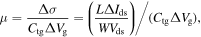
To evaluate electric behaviors of the fabricated FET sensors, we have measured the I–V curves, including Ids–Vg at different Vds (from 0.98 to 1.02 V with a step of 0.05 V) and Ids–Vds at different Vg (from 0 to 9.0 V with a step of 1.0 V). The transport characteristics of the FET are shown on figure 5. As seen in figure 5(A), as Vds increases, the minimum conductance point, where the type of charge carrier is changed, was shifted towards higher Vg values (see the arrow direction in figure 5(A)). Likewise, the inflection point was shifted to higher Vds as increasing Vg (see the arrow direction in figure 5(B)). The field effect carrier mobility (μ) turns out to be ∼7.21 cm2 V−1 s−1 via
where Δσ, L, W, ΔIds, Vds, ΔVg, and Ctg are the differential conductance, channel length, channel width, differential drain–source current, drain–source voltage, differential voltage and the total top gate capacitance, respectively. The total top gate capacitance (Ctg) can be calculated from the equation [17]

Figure 5. Electrical characteristics of the fabricated sensor. (A) Ids as a function of Vg for different Vds from 0.98 to 1.02 V with a step of 0.05 V; (B) Ids as a function of Vds for different Vg from 0 to 9 V with a step of 1.0 V. The dotted arrow shows the direction of the shift in the minimum of Ids; and (C) Ids versus Vg curves measured for different atrazine concentrations at Vds = 1.0 V. As the atrazine concentration increases, from 2 × 10⁻⁴ to 20 ppb, the minimum of Ids is shifted towards higher Vg.
Download figure:
Standard image High-resolution imageThe capacitance of the gate electrolyte (CEL) can be described from the equation
where r, h, ε0, εr are the radius of the graphene layer, the thickness of the gate insulator, the permittivity of free space, and the relative permittivity of the solution, respectively. For the electrolyte-gated GFETs (with r = 0.9 mm, h = 1 nm, ε0 = 8.854 × 10⁻¹² F m−1, εr = 80), the CEL is ∼3002 nF cm−2. With the quantum capacitance of the graphene channel (Cq) is approximately 2 μF cm−2 [14], the Ctg is 1200 nF cm−2. The mobility value of our graphene-based FET is smaller than that of other graphene—based FETs [17, 22].
3.3. Atrazine detection
For a perfect and contamination-free graphene devices, the minimum conductance point should be close to zero [22]. If the graphene surface adsorbs any chemicals, the minimum conductance point of graphene will be shifted towards positive or negative gate voltage. By observing the shift of the minimum conductance point, one can determine the change in behaviors of graphene surface [22]. Figure 5(C) shows the variation of drain–source current of FLG as function of the gate voltage at different concentrations of atrazine (from 2 × 10⁻⁴ to 20 ppb). The applied drain source voltage was 1 V. As the atrazine concentration increases from 2 × 10⁻⁴ to 20 ppb, the minimum conductance point (where the channel conductance is minimum [20]) was shifted towards higher values of Vg. As seen in figure 5(C), the value of current response (Ids) changed (from 6.456 to 6.709 mA) whereas the Vg at minimum conductance point shifted toward positive values as increasing concentration of atrazine (from 1.05 to 1.98). This result was also observed in other report [1]. The working principle of our atrazine biosensor is based on the inhibition of pesticide toward urease. In ion sensitive field-effect transistor biosensor, the conductivity of electrode surface is critical to determine the position, the intensity and the width of minimum conductance point. In our case, the hydrolysis of subtrate provided ions (NH4+, OH−) that would be adsorped onto electrode surfaces, then led to the increase in charge density and mobility on graphene layer [19]. Hydrolysis reaction:

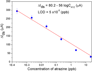
When atrazine is introduced, it acts as an inhibitor to reduce activity of enzyme, lowers the concentrations of ions at the electrodes and subsequently decreases current signal. The decrease of the differential drain–source current (ΔIds) with increasing atrazine concentrations expanding from 2 × 10⁻⁴ to 20 ppb was described in figure 6. Within the range of studied concentrations, the device showed good linearity with a coefficient of determination (R2) of 0.98. The regression equation was

Figure 6. The dependence of the differential drain–source current (ΔIds) on concentration of atrazine.
Download figure:
Standard image High-resolution image
The LOD and sensitivity were estimated to be 0.05 ppt and 56 μA/logC(ATZ), respectively. This value is much lower than detection limits for atrazine biosensors in previously reported works [27–33].The key of the performance achieved for the atrazine sensor described here must rely on the combination of CVD-grown Gr film and FET configuration. Compared to other graphene forms, CVD-grown FLGr films exhibits stronger and more controllable interaction with chemical/biological elements through π–π bond [17]. Also, it was reported that a synergistic effect in which electron transfer process was enhanced might occur at the edges of graphene planes [20]. Nevertheless, considerable works must still be done to gain better knowledge and insights on graphene materials that will advance the design of future graphene based sensing devices and improve their performances.
4. Conclusion
In conclusion, we have investigated a GFET enzymatic sensor for pesticide detection. The urease molecules were immobilized in a few-layered graphene channel between S and D electrodes. The inhibition of enzymatic hydrolysis of urea in presence of pesticide was captured as drain-source current changes. The sensitivity of graphene sheet—based FET atrazine sensor was 56 μA/logCATZ. The detection limit of atrazine sensor was determined to be 0.05 ppt. GFET devices will probably play a key role in the future biosensing systems that can electrically detect biomolecules with high sensitivity and specificity.
Acknowledgments
This research is funded by projects: VAST (VAST03.06/14-15, VAST.ĐLT.04/14-15, VAST.HTQT.NGA.10/16-17) and PICS-CNRS n° 6457.