


Abstract
In the proposed work an analytical model of a p-channel dual material gate all around tunnel FET (DMGAA-TFET) is presented and its performance is compared with the conventional GAA-TFET. The electrostatic potential profile of the model is obtained using 2-D Laplace's solution in the cylindrical coordinate system. A quantitative study of the drain current has been carried out using electric field in the z-axis and tunneling path. However the potential and current analysis is prolonged to different combinations of gate length in the DMGAA-TFET model. The results show an improvement in drain current and subthreshold swing as compared to GAA-TFET, which makes this model a potential replacement for low power application. Also the effect of scaling of the gate oxide thickness and cylindrical pillar diameter on the surface potential, initial tunneling point and tunneling current are analyzed.
Export citation and abstract BibTeX RIS

Original content from this work may be used under the terms of the Creative Commons Attribution 3.0 licence. Any further distribution of this work must maintain attribution to the author(s) and the title of the work, journal citation and DOI.
1. Introduction
As the conventional metal-oxide-semiconductor field effect transistor (MOSFETs) scaled beyond its physical limit, it suffers from high subthreshold swing (SS), high leakage current (IOFF) and other short channel effects (SCEs) like threshold voltage roll-off and drain induced barrier lowering (DIBL) [1–4]. Many researchers employed a number of multi-gate silicon on insulator metal-oxide-semiconductor (MOS) technology to improve the device performance by enhancing the gate control over channel from various sides [5–8]. However gate all around (GAA) MOS provides highest degree of control over channel and lowest characteristics length with the reduction of various SCEs compared to omega/pi-gate, tri-gate, double-gate and single-gate structures [9–11]. That also demonstrates the maximum scaling capability and strong electric field confinement of the structure. But the key concern of GAA-MOS device is that it offers high subthreshold swing and leakage current in the subthreshold region which makes the device incompatible for low power and steeper switching applications [12, 13].
GAA tunnel FET (TFET) is the likely alternative for MOS technology which has the capability to reduce SS limit and improve the device scaling performance. Also it reduces different SCEs because of gated p-i-n structure. The movement of charge carriers in TFET is due to the non-local band-to-band tunnelling (BTBT) process and is independent of temperature variation [14–18]. It also offers better electrostatic control over the channel due to cylindrical gate confinement [9]. A number of analytical models have been proposed to compute the potential and drain current of multi-gate TFET by using Kane's model [19–22]. However GAA-TFET provides low on-state drain current and high off-state leakage current compared to bulk technology due to tunnelling process [23]. The improvement of on-current in TFET can be achieved by optimizing the band-gap energy of semiconductors [24]. The gate engineering can be employed to enhance the tunnel current and to optimize the device parameters as proposed by Saurabh et al [25, 26].
In this paper a dual material gate all around TFET (DMGAA-TFET) analytical model is developed which has two regions with different work functions cascaded to each other. The region-1 is having higher work function as compared to region-2. The change in surface potential due to work function difference results in improvement of gate control over tunneling process and thus drain current increases compared to single material. The model provides high tunneling current with reduced DIBL and better scaling of oxide thickness and cylindrical pillar diameter. In this work the entire channel length is considered as 30 nm. The behavior of electrostatic potential and drain current for different combinations of gate length such as L1 = 10 nm and L2 = 20 nm, L1 = 15 nm and L2 = 15 nm, L1 = 20 nm and L2 = 10 nm are observed. The combination L1 = 20 nm and L2 = 10 nm shows better performance compared to other combinations. The effect of scaling of tox and tsi on electrical parameters is also studied.
2. Analytical model of DMGAA-TFET
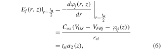
The cross-sectional view of a p-channel dual material GAA-TFET structure is shown in figure 1. The source and drain regions are heavily doped with pentavalent and trivalent impurity of concentration 1020 cm−3 respectively. The channel region is un-doped and made up of intrinsic material with negligible trivalent concentration of 1015 cm−3. For the given model two different metals having worked function  and
and  are considered as the gate metal contacts. The entire channel is divided into two regions (region-1 and region-2) as depicted in figure 1. The effective length of these non-overlapping channel regions are L1 and L2 respectively. However the low-k dielectric SiO2 is used as the gate oxide layer having thickness (tox) 2 nm. The diameter of silicon cylindrical pillar (tsi) is taken as 10 nm. Here the length of both metallic regions is varied keeping the work function and total channel length constant.

Figure 1. Schematic cross-sectional view and side-view of p-channel DMGAA-TFET.
Download figure:
Standard image High-resolution imageThe effect of doping concentration of channel on analysis of electrical parameters is neglected as the channel is considered as intrinsic and is lightly doped with a concentration of 1015 approximately. The electrostatic potential of both the channel regions have been obtained by solving the 2-D Laplace's equation which is obtained by neglecting the electron space charge.
Here  and
and  denote the electrostatic potentials in the channel region-1 and region-2 respectively. The above equation can be used to compute the surface potential at the gate-channel interface and center potential at the center of cylindrical pillar for both channel regions


The solution of above Laplace's equation in both regions has been resolved using 2nd order polynomial approximation [13]

The boundary conditions are required to predict the z-dependent coefficients 
 and
and  for both the regions. The electric field at the center of cylinder and gate-channel interface for both regions are [9]

where

Here  is the dielectric permittivity of silicon,
  is the oxide capacitance,
  is the permittivity of oxide layer and
  is gate-to-source bias. However
  denotes the flat-band voltage of both the regions, which is independent of gate length and can be calculated through the work function of materials

where  and
and  represents the work function of gate material for jth region and silicon work function respectively.
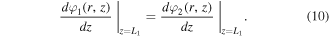
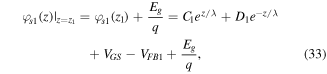
The essential boundary conditions at the interface of both the channel regions are required to solve equation (1). The potential profile and lateral electric field for both the regions are same at the interface

Using the above boundary conditions at the center of the cylindrical pillar, channel-SiO2 interface and dual region interface, the potential profile at the center is found to be
where λ is known as the natural length of cylindrical structure and is expressed as

The surface potential of the cylindrical structure  is related to the center potential
  as [25]

where

Differentiating equation (13), we get
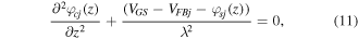
Now equation (11) becomes
The surface potential for both the channel regions are obtained by solving equation (16).
For region-1 

Similarly the surface potential for region-2,  is expressed as

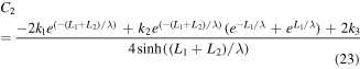
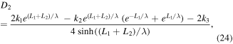
For the above expressions the coefficients C1, C2, D1 and D2 can be calculated using the potential boundary conditions at the source and drain end [27]


Here  is the built-in-potential,
  is the voltage applied at the drain terminal and
  is the maximum channel length of the device. Equating equations (17) and (18) using the boundary conditions at source-channel and drain-channel interface, we found
where


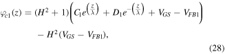
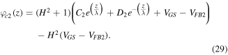
However the center potentials of both the channel regions can be obtained using equation (13). The center potentials of region-1 and region-2 are expressed as
In conventional TFET the tunneling of charge carriers is primarily based on is non-local BTBT mechanism [28–30]. For GAA-TFET the tunneling process is dominant in the lateral direction of cylindrical body. So it is desired to find the lateral field in both the channel regions which helps us to calculate the tunneling current. However the lateral electric fields in both the regions are obtained by differentiating the potential profile in the range of  and
and 
3. Drain current analysis
In non-local BTBT the tunneling of charge carriers starts only when the conduction band of source gets in-line with the valence band of channel region [31]. At zero gate bias a small amount of band bending arises at the source-channel interface, because of the presence of built-in-potential. This condition is known as OFF-state condition of the device as depicted in figure 2(a). In this state the current in the channel is insignificant due to the absence of band-to-band tunneling. Further increase of gate bias results significant amount of band bending. When the applied gate potential attains a critical value (Vth), the conduction band of source and valence band of channel gets aligned to each other. For VGS > Vth, the drain current increases exponentially due to the improvement in tunneling volume as depicted by the area under the solid lines in figure 2(b).

Figure 2. Energy band diagram of p-channel DMGAA-TFET in (a) OFF-state and (b) ON-state.
Download figure:
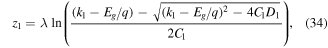
Standard image High-resolution imageIn the ON-state the tunneling path is the lateral distance between the two tunneling points z1 and z2. The initial tunneling point is the value of z for which the surface potential changes by an amount of unit band gap energy per elementary charge  However this point plays a decisive role in the extraction of drain current. In this model z1 is assumed to lie in the region-1
  because the region-1 is surrounded by the metal with higher work function. So the tunneling distance z1 can be obtained by using the surface potential profile at the interface and at the critical threshold point

where  is the band-gap energy of silicon at equilibrium.
  can be further reduced by optimizing band-gap energy of semiconductor and increasing the gate potential (VGS). Low
  increases the tunneling path along the channel and hence the drain current is improved. In this model the tunneling volume is not affected by the drain voltage for constant VGS. This is because the effect of electron charge injected into the channel from the drain end has been neglected in equation (1).
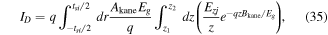
The drain current can be calculated by integrating BTBT generation rate over the entire tunneling volume in both the radial and lateral directions. However, for the present model the current is obtained in the lateral direction of channel from  to
to  using Kane's direct tunneling phenomena [32]. Here
  lies in the region-1 due to sharp reduction of the surface potential and
  lies in the region-2 due to charge accumulation at drain end as shown in figure 2(b). So the drain current is expressed as
where  and
and  are tunneling dependent Kane's parameters having values:
  = 4 × 10¹⁵ m−1/2 V−5/2 s−1 and
  = 1.9 × 10⁹ V m−1 [33].
On simplifying equation (35), we get

Here both the channel regions involve tunneling process as  and
and  Hence the tunneling volume is calculated by integrating the generation rate over both regions and is expressed as
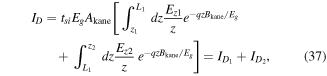
where  and
and  are the drain current in the channel region-1 and region-2 due to non-local tunneling process. Substituting the value of lateral electric field of both regions, we get
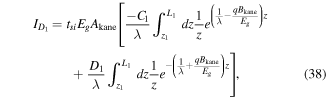
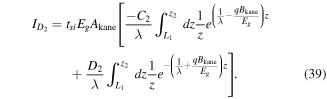
In the above integration process, the effect of the exponential term in numerator is dominant as compared to the polynomial term in denominator. So the drain current is obtained by integrating equations (38) and (39) between the two tunneling points by neglecting the effect of the polynomial term
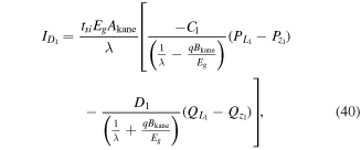
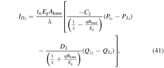
where


In equation (41) the exponential parameter  and
and  for
for  So neglecting the nominal effects of
  and
and  in the drain current analysis, we found
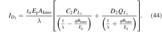
The final drain current expression is obtained as
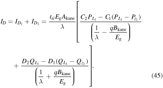
4. Results and discussion
Figure 3 shows the variation of surface potential along the 30 nm channel for single material and dual material gate. The gate lengths of both the regions are varied and their impact on potential is observed. The dual material having L1 = 20 nm and L2 = 10 nm produces minimum surface potential and sharp slope as compared to other combinations. This is because of higher work function and larger gate length of the region-1. The sharp reduction of potential is responsible for increase of the BTBT tunneling volume and drain current. So for this model, current analysis has been done with gate length L1 = 20 nm, L2 = 10 nm and results are compared with different combinations of dual gate lengths.

Figure 3. Surface potential distribution of GAA-TFET with single material gate and dual material gate for 30 nm channel length and −0.1 V drain voltage.
Download figure:
Standard image High-resolution imageThe center potential at r = 0 and surface potential at r = tsi/2 of the DMGAA-TFET are compared for different gate voltages in figure 4. For a constant gate voltage the center potential lies above the surface potential. This is due to higher influence of gate bias at the channel interface. In the present analysis surface potential based approach is followed for the calculation of tunneling current.

Figure 4. Electrostatic potential along the channel at the center and surface of DMGAA-TFET.
Download figure:
Standard image High-resolution imageThe surface potential profile for the proposed model with different gate voltages at a constant drain voltage are illustrated in the figure 5(a). The potential is stuck to built-in-potential (Vbi) at the source interface and VDS at drain interface as per the boundary condition. The surface potential in both the channel regions reduces with increase in gate voltage at VDS = −0.1 V. Therefore the slope of the surface potential is getting sharper and the minimum potential is achieved early. The sharp slope of the potential for higher gate voltage indicates the larger tunneling volume. However the potential of entire channel of GAA-TFET varies linearly. This is due to the impact of drain bias over both the channel regions. Figure 5(b) shows the surface potential of the proposed device for various drain voltages. It is observed that the slope of the reduced potential profile is not affected by the increment of the drain voltage as the effect of electron space charge has been ignored in equation (1). Hence there will be no significant drain induced barrier lowering (DIBL) effect in the model, so the tunneling current is not affected by drain bias.

Figure 5. Variation of surface potential along the channel at different (a) gate voltages and (b) drain voltages.
Download figure:
Standard image High-resolution imageFigure 6 demonstrates the effect of reducing gate oxide thickness and pillar diameter on the surface potential and the results are compared to the conventional GAA-TFET. Unlike the orthodox model, the potential of DMGAA-TFET decreases as we go on reducing tox and tsi. The potential is minimized further due to the influence of gate bias on channel at low oxide thickness and pillar diameter. Dual material GAA-TFET shows reduced and sharp slope potential profile as compared to single material gate.

Figure 6. Surface potential distribution of the model with single material gate and proposed dual material gate along the channel due to the variation of (a) gate oxide thickness and (b) cylindrical pillar diameter.
Download figure:
Standard image High-resolution imageFigure 7 shows the behavior of lateral electric field of the model and that has been compared with the different combinations of gate length. It is clearly seen that the electric field varies non-linearly for the entire channel for a constant gate and drain bias and the field exists for both the channel regions. However the lateral field plays a vital role in the calculation of tunneling volume over the entire channel.

Figure 7. Lateral electric field along the channel length of the device with single material gate and different length based dual material gate.
Download figure:
Standard image High-resolution imageThe initial tunneling points for different values of gate length as a function of gate voltage are shown in figure 8. The results are compared to the conventional GAA-TFET. As the gate voltage increases beyond threshold, the charge carriers tunnel from source to channel which results  Lower the
  better the tunneling volume. Inclusion of dual material gate results in low
  hence improves the device performance. For the proposed model the combination of the gate lengths L1 = 20 nm and L2 = 10 nm yields best result because of sharp slope of surface potential. The sharp reduction of surface potential reduces threshold voltage, hence achieves tunneling earlier.

Figure 8. Variation of initial tunneling point (z1) versus gate voltage for different combinations of gate length.
Download figure:
Standard image High-resolution imageFor a constant gate oxide thickness and cylindrical pillar diameter,  reduces with increase in gate voltage beyond threshold. As the gate oxide thickness (tox) is scaled from 3 to 1 nm for radii of 5 nm, more tunneling volume is achieved because of the reduction of
  as depicted in figure 9(a). This is due to the impact of gate bias on channel with low oxide thickness. Reduction in
  enables the flow of charge carriers for small value of VGS. Similarly figure 9(b) displays the variation of
  versus VGS for different Si pillar diameter for the dual material model. When the diameter of cylindrical pillar reduces, the gate control on the channel is dominant and thereby reduces
  marginally. Therefore the scaling of tox and tsi improves the drain current performance of DMGAA-TFET.

Figure 9. Impact of (a) gate oxide scaling and (b) cylindrical pillar diameter scaling on initial tunneling point (z1) versus gate voltage.
Download figure:
Standard image High-resolution imageFigure 10 shows ID-VGS characteristics for GAA-TFET in linear and logarithmic scale. The drain current analysis is done for different combinations of gate length as a function of gate voltage. As the gate bias increases beyond threshold, the tunneling current flows from source to drain end along the lateral direction. However the on current performance of dual material gate is better as compared to single material, because of sharp potential reduction and minimum threshold achievement. Here also the gate length combination L1 = 20 nm and L2 = 10 nm yields better performance in comparison with other lengths as the BTBT current primarily influenced by the sharp potential profile near the source-channel interface. The drain current improves exponentially for VGS > Vth due to dominant tunneling process in both channel regions. Figure 10(b) displays the logarithmic drain current versus VGS. The model produces drain current in the range of 10−5 A compared to single gate model (10−6 A) depicted in figure 10(b). High ION and low IOFF can be achieved because of large L1 and small L2, respectively. So the gate length combination L1 = 20 nm and L2 = 10 nm provides maximum ION to IOFF ratio.

Figure 10. Characteristics of drain current ID versus gate voltage VGS for p-channel GAA-TFET with single-material and dual-material gate. The drain current is plotted on (a) linear scale, (b) logarithmic scale.
Download figure:
Standard image High-resolution imageThe ID-VDS characteristics for different gate length combinations are shown in figure 11(a) at constant gate bias. In the ON state the drain current is independent of drain voltage, because of the dominancy of gate bias. The independent nature of drain current versus VDS is due to the fact that the electron space charge has been neglected in the electrostatic potential analysis. At VGS = −1 V, the conventional GAA-TFET produces current of order 10−10 A. This negligible amount of current resulted, because at VGS = −1 V the device operates at cut-off. Whereas with the same gate voltage DMGAA-TFET yields higher drain current of order 10−8 A with low threshold. However the device with higher region-1 dimension gives better on current performance at constant gate voltage. Figure 11(b) shows the ID-VDS characteristics of DMGAA-TFET for different gate voltages. It is clearly observed that increase in gate voltage beyond threshold results increment in drain current.

Figure 11. Characteristics of drain current ID versus drain voltage VDS for the model (a) with different gate length combination in dual-material gate at constant gate voltage, and (b) with fixed gate length in dual-material gate for different gate voltages.
Download figure:
Standard image High-resolution imageFigures 12(a) and (b) display the effect of tox and tsi variation on drain current. Figure 12(a) shows significant increment of drain current with reduction in oxide thickness for the model, because of the small value of initial tunneling point. This leads to larger tunneling volume in non-local direct tunneling process and hence results large tunnel current. Similarly the effect of scaling of tsi on drain current for different combinations of gate length is depicted in figure 12(b). It is clearly observed that high drain current is obtained at lower thickness of the cylinder due to higher influence of gate on channel. The BTBT tunneling takes place faster for small diameter and conversely improves the tunneling current. Comparing the results for different combinations of gate length, L1 = 20 nm and L2 = 10 nm gives better performance. Figures 13(a) and (b) show the effect tsi and tox scaling on ID versus VGS characteristics of DMGAA-TFET and concluded that higher drain current is achieved at low tox and low tsi due to gate-dominant tunneling process. As we scaled down the tsi from 10 to 6 nm, the tunneling current improves by a factor of 10 as given in figure 13(a). However in the subthreshold region (VGS < Vth), the effect of the variation of tsi is insignificant on drain current due to the absence of tunneling of carriers.

Figure 12. Impact of (a) gate oxide tox and (b) cylindrical pillar diameter scaling tsi on drain current ID.
Download figure:
Standard image High-resolution image
Figure 13. Effect of (a) cylindrical pillar diameter, and (b) gate oxide variation on characteristics of drain current ID versus gate voltage VGS for the proposed model.
Download figure:
Standard image High-resolution image
Subthreshold swing (SS) can also be calculated for different gate voltages in the subthreshold region and compared to single-material GAA-TFET as shown in table 1. DMGAA-TFET produces low SS for VGS < Vth.
Table 1. Comparison of subthreshold swing for different models.
| VDS(V) | tox(nm) | tsi(nm) | Subthreshold swing (mV/decade) | |||
|---|---|---|---|---|---|---|
| GAA-TFET L = 30 nm | DMGAA-TFET L1 = 10 nm, L2 = 20 nm | DMGAA-TFET L1 = 15 nm, L2 = 15 nm | DMGAA-TFET L1 = 20 nm, L2 = 10 nm | |||
| −1 | 2 | 10 | 44 | 38 | 40 | 36 |
| −1 | 2 | 8 | 40 | 34 | 38 | 32 |
| −1 | 2 | 6 | 38 | 34 | 34 | 30 |
Therefore this model can be a potential candidate for ultra-low power CMOS applications in the near future due to vast improvement of drain current at low subthreshold swing.
5. Conclusion
In this paper a 2-D analytical model for p-channel DMGAA-TFET is developed. The work proposes the potential profile of two channel regions for different gate length ratios. This results improved drain current compared to conventional GAA-TFET. The impact of work function, gate length, gate oxide thickness and cylindrical body diameter on the drain current and initial tunneling point are discussed. The drain current is improved approximately by a factor 10 for DMGAA-TFET compared to conventional GAA-TFET. Also the improved SS resulted for the present model (30 ∼ 40 mV/decade) allows the device to be a promising candidate for low power and high speed application.