

Abstract
This paper will present the unique characteristics of aluminum oxide (Al–O) and cobalt catalyst included in aligned carbon nanotube (CNT) electrode system of energy storage device, namely electrochemical capacitor. Electrical conductivity and nanostructure of the thermally oxidized Al–O used as catalyst-support layer in vertically grown single-walled CNTs were studied. Al–O films were characterized by means of current–voltage measurement and high resolution transmission electron microscopy analysis. The Al–O support layer was found to be conductive, with a relatively low resistance and, approximately 20 nm film thickness of Al–O is suggested to be too thin to form insulating barrier. The scanning TEM—annular dark field analysis confirmed that the nanosized cobalt catalyst particles distributed on Al–O surfaces and also embedded inside the Al–O film structure.
Export citation and abstract BibTeX RIS

Original content from this work may be used under the terms of the Creative Commons Attribution 3.0 licence. Any further distribution of this work must maintain attribution to the author(s) and the title of the work, journal citation and DOI.
1. Introduction
Carbon nanotubes (CNTs) have attracted so much attention from materials scientists all over the world due to their special dimension and structures. In practice, contrary to the random forms of CNTs on substrates, aligned or well organized CNT arrays offer many advantages for a wide variety of applications [1]. For more than two decades, catalytic chemical vapor deposition has been the most popular method to grow aligned CNTs due to its economical factor and wide selection of materials (substrates, catalysts). Metal based oxides especially aluminum oxide (Al–O) and alumina (Al2O3) are mostly selected for catalyst support layers. The CNT formation strongly depends on catalytic activity, catalyst lifetime, and the most crucial factor is the function of catalyst-support materials to align the CNTs [2, 3]. The surface condition of these metal oxides is viable to support metal catalyst nanoparticles during chemical vapor deposition (CVD) process [4–7].
One of the most demanding applications of aligned CNTs is their usage in energy storage devices (electrochemical capacitors, batteries etc). Nowadays aligned CNTs are focused as active/electrode material by researchers in the field of applied electrochemistry due to their advantages in specific surface area and electrolyte ion accessibility [8–10]. As compared to that of random or non-aligned form of CNTs, aligned structure of CNT in principle can assure more electrolyte ions to access the surfaces of the material, and thus may increase the charge storage ability [11]. Among the carbonaceous materials, CNT based supercapacitor demonstrated better charge/discharge ability, because CNT intrinsically exhibits superior electric conductivity and mesoporosity [12, 13].
Previously various electrochemical measurements proved that vertically aligned-single walled carbon nanotubes (VA-SWCNTs) had excellent electrical contact with current collector—SUS 310S foil [8, 14]. The success in ensuring the working ability of electrochemical capacitors confirmed that Al–O used to support Co in growing vertical CNTs is conductive (non-insulating). The clarification for the conductivity of Al–O support layer is crucial in order to understand the mechanism of VA-SWCNT charge storage contribution. Hence, it is important to clarify the above-mentioned idea.
In this work the resistivity of Al–O thin film had been studied by current–voltage (I–V) measurement to clarify the electrical conductivity of sample used in electrochemical capacitor. The morphology at nanoscale level of Al–O incorporated with Co catalyst nanoparticles was also studied to further understand the origin of the film's conductivity.
2. Experimental
The Al thin films of 20 nm nominal thickness were deposited using electron beam physical vapor deposition (EBPVD) at 10−4 Pa. The deposition rate (constant at 0.1 nm s−1) was monitored by a quartz resonator. The temperature of substrate during EBVPD process was kept constant at less than 200 °C, low enough to not affecting the morphology of the Al films. The thickness monitor of quartz resonator was calibrated using Alpha-Step500 surface profiler and atomic force microscopy.
For the formation of thermally-oxidized Al–O, deposited Al was first naturally-oxidized at room temperature for 2 h. Then, the substrate subsequently transferred to CVD reactor and oxidized at oxidation temperature (Tto) of 400 °C in static air for 10 min. For comparison and clarity, Al–O coated with 0.5 nm nominal thickness of Co (Co/Al–O) was prepared and then further annealed at TCVD (700 °C–750 °C, Ar/H2) for 5 min. Electric furnace (MILA-3000) was employed as the CVD reactor for CNT growth. Experimental details of Al–O film preparation and CNT growth using alcohol catalytic CVD in similar laboratory can be found elsewhere [8].
In the I–V measurement, a SUS 310S conducting foil, which has been used as current collector of electrochemical capacitor was used as substrate. All substrates used in this work were rinsed with acetone before undergone ultrasonic bath cleaning in ethanol for 10 min.
Two-probe I–V measurements were carried out using Agilent 4155C semiconductor parameter analyzer under ambient condition (figure 1). I–V characteristics were obtained by placing thin Au foil (5 × 5 mm2 area) on the top surface of the samples. A tungsten (W) probe was connected to SUS 310S foil and the other probe was connected to a soft Au thin wire and placed on the Au foil. Repeated cycles of measurements were performed to check the consistency of the data.
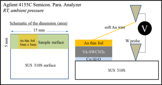
Figure 1. Schematic of I–V measurement for the confirmation of electrical conductivity of substrates prepared using Al–O films.
Download figure:
Standard image High-resolution imageFor transmission electron microscopy (TEM) observation, Si (100) wafer with thermal oxide layer (400 nm) was used as substrate. It is important to note that the usage of either SUS 310S foil or Si wafer may result in similar thin films characteristics, and similar CNT growth performance. High resolution morphological analyses of Co/Al–O sample at high resolution were carried out by using field emission TEM (FE-TEM, JEOL JEM-2100F) which equipped with a beam-scanning for scanning TEM (STEM) analysis. The maximum magnification used for this analysis was 390 000 times. TEM samples were prepared by using Ar ion milling method (Gatan Model691) for plane-view analysis, and focused ion beam (FIB, Hitachi FB2000A) for cross-sectional analysis.
3. Results and discussion
3.1. Electrical conductivity of Al–O support layer used for VA-SWCNT growth
As explained in experimental procedure, Al and Co films were deposited on SUS 310S using EB-deposition to prepare three different measurement samples, namely Al–O, Co/Al–O, and VA-SWCNT/Co/Al–O. During the preparation of VA-SWCNT/Co/Al–O sample, 50 μm thick of VA-SWCNTs was directly-grown from Co/Al–O (figure 2). Significant results of VA-SWCNT growth covering the optimization of CVD parameter and materials characterization were discussed in previous studies [8, 14, 15].
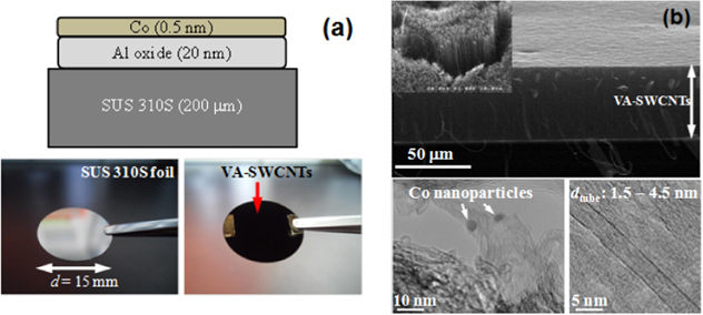
Figure 2. VA-SWCNT growth on SUS 310S foil. (a) Digital image of SUS 310S foil, with and without VA-SWCNT forest. (b) SEM and TEM images of SWCNTs. (reused with permission from Wiley [8]).
Download figure:
Standard image High-resolution imageI–V curves of all three samples measured at room temperature are shown in figure 3 and the results are tabulated in table 1. The contact resistance is assumed to be similar for all samples. From I–V measurement, electrical resistivity ρ (Ω m) can be estimated from the resistance R (Ω) using formula

where l is the thickness of Al foil + VA-SWCNT + Co/Al–O, and A is the cross-sectional area of the sample area of Au foil (m2). Furthermore, the electrical conductivity σ (S m−1) which defined as the inverse of resistivity can be directly calculated using relation


Figure 3. Confirmation of Al–O film electrical conductivity using I–V measurement. The samples are thermally-oxidized Al–O (black), further-annealed Co/Al–O (blue), and VA-SWCNT/Co/Al–O (red).
Download figure:
Standard image High-resolution imageTable 1. Calculated electrical conductivity of thermally-oxidized Al–O.
| Sample | R (Ω) (from I–V curve) | ρ (Ω m) | σ (S m−1) |
|---|---|---|---|
| Al–O (thermally-oxidized) | 283 | 3.54 × 10⁵ | 2.83 × 10⁻⁶ |
| Co/Al–O (further- annealed) | 272 | 3.32 × 10⁵ | 3.01 × 10⁻⁶ |
| VA-SWCNT/Co/Al–O | 299 | 150 | 6.69 × 10⁻³ |
As a result, the conductivity of Al–O films was confirmed by the linear relation of I–V characteristics for both samples with and without VA-SWCNTs (figure 3). In addition, almost similar resistance values obtained from the linear curves. The calculated electrical conductivity of thermally-oxidized Al–O (table 1) shows an increase to more than four magnitudes compared to pure alumina [16]. The conductivity of Al–O is slightly higher than that of bulk alumina. It can be hypothesized that the Al–O thickness of 20 nm is too thin that made the resistance to be relatively low, therefore gives the ohmic resistance behavior.
The properties of Al–O become size-dependent due to the surface effect and quantum confinement effect [17]. There are a few reasons that might possibly cause the Al–O thin film to obtain ohmic resistance behavior, namely the Coulomb charging and tunneling mechanism as well as change of microstructures [18]. Tunneling involve the charge transport through an insulating medium separating the conductors that are closely spaced. This is because the electron wave functions from the conductors overlap inside the insulating material when the thickness is extremely thin. Meanwhile, the formation of ordered microstructure when the size is reduced to nanoscale may attribute to the change in electrical conductivity. Another possible reason for the change in electrical conductivity is the insulator–metal transition, also known as Mott transition [19]. This transition allows the material to switch from electrical insulator to electrical conductor. The insulator–metal transition is modified by the changes in temperature, pressure or composition (doping).
As in the case of Al–O thin film, the nanosize caused the high concentration of defects which attribute to the doping mechanism. This is in agreement with the result of VA-SWCNT grown from Co supported by Al–O thin film where the resistance (299 Ω) is slightly lower than MWCNTs directly-grown on Inconel without Al–O (387 Ω) [20]. Hence, for electrochemical devices, the Al–O film of up to 30 nm thickness was reported to be too thin to form an insulating barrier on the metal foils, and with appropriate height of densely aligned CNT array, Al–O is hardly to affect the electronic conduction [21–24]. Furthermore the Al–O film did not influence the electrical contact between the VA-SWCNTs and the foil.
Another acceptable idea for the conductivity is that the Co catalyst particles remained metallic even after further annealed at CVD temperature [25]. Furthermore, a low resistance ohmic contact allows electrical charges to flow in both directions between SWCNT and SUS foil and thus giving the linear relation of I–V curve. This particular argument needs further investigation, but at this stage, it may summarize that all materials being used including VA-SWCNT forest do not affect electrical conductivity of the sample.
3.2. TEM observation of Co/Al–O substrate system
The morphological characteristic of Al–O thin film when incorporated with Co catalyst will be discussed by using TEM image of cross-sectional view of Co/Al–O on Si wafer after being further annealed at VA-SWCNT growth temperature of 750 °C (figure 4). The EB-deposited Al–O film was not so uniform, but the thickness is in the range of approximately 20 nm (figure 4(a)) considerably acceptable in order to support catalyst for vertical CNT growth. Also, Al–O film thickness in the figure shows a good agreement to those approximated and calculated in the study of x-ray photoelectron spectroscopy (XPS) and spectroscopic ellipsometry [26]. The black dots appeared in the figure are the Co catalyst particles.

Figure 4. (a) Cross-sectional TEM image of Co(0.5 nm)/Al–O(20 nm)/SiO2/Si substrate. Scale bar: 50 nm (390 000× magnification). Lower part: cross-sectional STEM-ADF images of Co(0.5 nm)/Al–O(20 nm)/SiO2/Si substrate. (b) Spectrum image and (c) enlarged image. Scale bar: 50 nm and 10 nm, respectively.
Download figure:
Standard image High-resolution image
Previous characterization of Al–O using x-ray diffraction and XPS showed that the Al–O has a non-crystallized structure and is non-stoichiometric in term of oxidation state [15]. The morphology of Al–O film in the figure can be considered as amorphous as the amorphous structure for an oxide film on metal substrate can be more stable than that of crystalline structure [27]. From the fact that crystallized and stoichiometric alumina (Al2O3) is normally insulating, amorphous Al–O might have made the system to have an electrical path for electron transfer from SUS foil to Co and CNTs.
On the other hand, enhanced analysis on the cross-sectional view of scanning TEM annular dark-field (STEM-ADF) images of similar sample shown in figure 4(a) was carried out. STEM-ADF measurement is demonstrated for acquiring Z-contrast images at atomic resolution; thus, it is possible to form atomic resolution images where the contrast is directly related to the atomic number [28, 29]. In STEM-ADF image, the brightness (image intensity) is proportional to the atomic number, therefore, the black particles seen in the TEM image is observed as white particles. Therefore, white particles observed are corresponding to the distribution of Co catalyst particles (figures 4(b) and (c)). Co catalyst particles are not only appeared at the surfaces of Al–O and/or at Co/Al–O interfaces, but some of them are embedded inside the Al–O structure.
It can be suggested that catalyst particles distribution at the different support layer film might produce different scenario of CNT growth result. The existence of Co particles at Al–O interface caused the film to be electrically conductive. Future investigation of Co particle distribution on thermally oxidized Al–O film to clarify VA-SWCNT growth mechanism will be another interesting feature to be investigated.
4. Conclusions
Al–O support layer used for VA-SWCNT growth was prepared by the deposition of Al metal film and was thermally oxidized to make them suitable to support Co catalyst during CNT growth. Three different samples (Al–O, Co/Al–O, and VA-SWCNT/Co/Al–O) were prepared to confirm Al–O film electrical conductivity. As results, Co/Al–O substrate system used in this study was found to be conductive, and approximately 20 nm thickness of Al–O was too thin to form insulating barrier for a device. Cross-sectional TEM image confirmed the thickness of Al–O, and the STEM-ADF analysis clearly confirmed the nanosized Co particle distribution on Al–O surfaces, Co/Al–O interfaces, and also embedded inside the Al–O structure. This information confirms the electrical conductivity of the film and thus made the structures good to use in electrochemical capacitors.
Acknowledgments
This work was supported by a Grant-in-Aid from Japan Society for the Promotion of Science (JSPS), and Science Fund research grant from Ministry of Science, Technology and Innovation (MOSTI), Malaysia numbered 03-01-14-SF0063. Special thanks to Dr K Fukada (JAIST Green Device Research Center) for sharing his expertise in I–V measurement. Authors are also thankful to Kobelco Research Institute, Inc., Japan for HRTEM analysis support.