

Abstract
The present work is devoted to the review of the methods to improve light trapping into polymer solar cells. After a discussion on the important role of the improvement of the light-trapping technique in the fabrication of solar cells by applying the plasmonic enhancement effect, we review the results of the study on this topic, which were obtained mainly during recent years. The light-trapping nanostructures usually comprised the following basic elements: antireflection coating, randomly distributed or symmetric–periodic monolayers of metallic spherical nanoparticles (NPs), metallic NPs with different shapes, spherical NPs with core–shell structure, nanovoids, plasmonic metallic grating, grating organic active layer, grating indium tin oxide (ITO) layer, dielectric grating, photonic structure, and plasmonic cavity with subwavelength hole array. Each light-trapping nanostructure may use either one or two of the above-mentioned basic elements.
Export citation and abstract BibTeX RIS

Original content from this work may be used under the terms of the Creative Commons Attribution 3.0 licence. Any further distribution of this work must maintain attribution to the author(s) and the title of the work, journal citation and DOI.
1. Introduction
The study of plasmonic enhancement of photocurrents in photovoltaic devices was initiated by Stuart and Hall since the last years of the past century [1]. These authors have demonstrated that a photocurrent enhancement of a factor of 18 could be achieved in a silicon-on-insulator (SOI) photodetector with a thickness of 165 nm at the wavelength of 800 nm by depositing silver nanoparticles (AgNPs) on the surface of the device. In a subsequent work [2] Schaadt et al investigated the enhanced optical absorption of a semiconductor by surface plasmon excitation and observed an enhancement of up to 80% at wavelengths around 500 nm when AuNPs were deposited on highly doped wafer-based solar cells.
Considering the enhancement of the light absorption by amorphous silicon solar cells via the scattering from surface plasmon polaritons in nearby metallic NPs, Derkacs et al [3] achieved an 8% overall increase of light-energy conversion efficiency. For the study of surface plasmon-enhanced Si solar cells, Pillai et al [4] investigated thick SOIs, as well as planar wafer-based solar cells deposited by AgNPs, and achieved an overall photocurrent increase of 33% and 19%, respectively. On the other hand, metal NPs can also be used to increase the efficiency of light-emitting processes. Indeed, Pillai et al [5] have also demonstrated overall electroluminescence enhancement with a factor of seven for thin SOI light-emitting diodes. Plasmonic enhancement of solar energy conversion in organic bulk heterojunction photovoltaics was investigated by Morfa et al [6]. An increase of efficiency by a factor of 1.7 was observed. Konda et al [7] studied the surface plasmon excitation via AuNPs in n-CdSe/p-Si heterojunction diodes and also observed an increase of the photocurrent. In reference [8] Catchpole and Polman investigated light scattering from a single Ag or Au particle, varying the shape, size, particle material, and dielectric environment in order to determine some fundamental design principles for particle plasmon-enhanced light trapping. They showed that cylindrical and hemispherical particles were much more effective than spherical particles at scattering light into a high-index substrate and keeping the light trapped within the substrate due to enhanced near-field coupling.
Due to the high cost of crystalline semiconductors there arose a great attention to the study of thin-film solar cells with thicknesses in the range of 1–2 μm on cheap substrates such as glass, plastic, and stainless steel. The semiconductor materials to be used to prepare thin-film solar cells were amorphous, as well as polycrystalline silicon and semiconductor compounds such as CdTe, CdSe, CuISe, etc However, the absorbance of semiconductor thin films is low, particularly for indirect bandgap silicon. Therefore it is very important to design the solar cells such that the light is trapped inside in order to increase the absorbance. For this purpose a very efficient method was proposed for enhancing the light absorption of solar cells by using the light scattering from Ag- or AuNPs excited at their surface plasmon resonance.
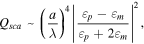
Besides the scattering of light by metallic NPs, the light absorption by metallic NPs also simultaneously took place. Catchpole and Polman [9] have noted that for particles with diameters well below the wavelength of light, the absorption and scattering of light are well described by the corresponding cross sections

where α is the polarizability of the particle

V is the particle volume, εp is the dielectric function of the particle, and εm is the dielectric constant of the embedding medium. When εp = −2εm the particle polarizability becomes very large. This is known as the surface plasmon resonance. At this resonance the scattering cross section can exceed the geometrical cross section of the particle. In the Drude model of metal

where ωp is the bulk plasmon frequency. Therefore

It follows that the surface plasmon frequency is

The above-presented initial works have promoted the subsequent rapid development of research to improve the solar cells by using the plasmonic enhancement. Reviewing the main results of this development is the purpose of the present article.
In the interesting work of Nakayama et al [10] the plasmonic enhancement of the photocurrent in a GaAs solar cell of 110 nm diameter AgNPs was investigated. The shape and density of the AgNPs were uniformly and systematically controlled using anodic aluminum oxide (AAO) templates. Annealing AgNPs yielded blue-shifted localized surface plasmon resonances (LSPRs), which were attributed to improvements in the symmetry of the NP shapes. After annealing, both the dense and sparse arrays of lower-aspect-ratio AgNPs have the peaks at similar wavelengths, while the dense array of higher-aspect-ratio AgNPs has a blue-shifted peak relative to the sparse array, implying the strong electromagnetic interaction in the dense array of higher-aspect-ratio AgNPs.
The authors have investigated all four types NP arrays: dense array of low-aspect-ratio (DL) NPs, sparse array of low-aspect-ratio (SL) NPs, dense array of high-aspect-ratio (DH) NPs, and sparse array of high-aspect-ratio (SH) NPs. The photovoltaic properties of the GaAs solar cells were studied. The arrays had significant influence on the photocurrent of the cells, and the best photocurrent enhancement was induced by the DH array, with an 8% increase of the short-circuit current density. The photocurrent loss/gain ratios relative to the reference cell were: 9%/12% for the DL cell, 4%/10% for the SL cell, 14%/26% for the DH cell, and 7%/7% for the SH cell, calculated from the external quantum efficiency equation under AM 1.5G illumination. The performance of plasmonic solar cells depends not only on the plasmonic enhancement by individual metallic NPs, but also on the design of arrays of these NPs for the optimum trapping of the light.
In reference [11], devoted to the study of the design of metal NP periodic arrays for light-trapping (LT) applications in solar cells, Mokkapati et al studied the effect of particle dimensions and grating pitch, as well as fill factor, and presented essential criteria of optimizing the LT efficiency of periodic arrays of AgNPs in Si solar cells. The authors have demonstrated that for efficient LT, the optimal geometry of the metal NP array is relatively narrowly defined due to the limited range of particle sizes, resulting in efficient light scattering into the substrate in the long wavelength range. This is in contrast to dielectric gratings, where a relatively wide range of periods and feature sizes can be used. The authors have shown that for efficient LT using periodic arrays of metal NPs, the particle dimensions and the dielectric environment should be chosen such that the dipole oscillation resonance belongs to the wavelength range of interest. It is also necessary to tune the grating parameters so that high diffraction efficiency is obtained in a wavelength range close to the dipole oscillation resonance of the individual particles, ensuring that most of the incident power is retained in the Si. The pitch of the grating should be chosen to allow at least one diffraction mode propagating outside the escape cone in Si for long-wavelength light. This imposes a lower limit of ∼400 nm on the grating pitch. In addition, a minimum fill factor of ∼20% should be maintained for efficient interaction between the incident light and the NP array. Taken together, these conditions place strong constraints on the optimal particle size and grating parameters. The authors conclude that arrays of particles with particle dimensions of ∼200 nm and a pitch of ∼400 nm are ideal for efficient LT in Si solar cells.
The basic design rules for the use of metallic nanostructures to realize broad-band absorption enhancement in thin-film solar cells were elaborated by Brongersma et al [12]. These rules are applied to a relevant model system consisting of a two-dimensional periodic array of Ag strips on a silica-coated Si thin film supported by a silica substrate. The authors illustrated a straightforward and physically intuitive procedure to optimize the net overall absorption by a thin-film Si solar cell over the entire solar spectrum, simultaneously taking advantage both of the high near-fields surrounding the nanostructure close to the surface plasmon resonance frequency and effective coupling to waveguide modes supported by the Si film through the optimization of the array properties.
The choices for the individual components of the cell structure were clarified as follows. The metal-strip geometry was chosen because of its simple cross-sectional shape, which is described by just two parameters (thickness and width). These strips can effectively concentrate the light in their vicinity at frequencies near their surface plasmon resonance. This resonance frequency critically depends on the strip geometry and its dielectric environment. It was well established that strong absorption and less scattering were caused by deep subwavelength particles as compared to the larger particles. Thus no significant benefit from light scattering and trapping can be expected from very small strips. Beneficial effects on the short-circuit current were provided by strips with characteristic sizes in the range of 50–100 nm. Substantially large strips behave like optical mirrors, reflecting most of the incident radiation back into free space. In contrast to the near-field concentration effects, the lateral spacing of the strips governs the excitation of waveguide modes. The number of allowed waveguide modes and their dispersion are determined by the thickness of the Si layer, and this important parameter should be chosen carefully. The SiO2 layers offer high optical transparency and can provide for excellent electrical surface passivation of the Si. The top oxide also serves as a spacer layer between the metal and the absorbing Si layer, whose thickness can be controlled with extreme precision using thermal oxidation.
In reference [13] Atwater, Polman et al demonstrated the improved red response of the n-i-p amorphous hydrogenated silicon (a-Si:H) solar cells with plasmonic back reflectors. The authors utilized nanoimprint lithography to pattern the back contacts of these solar cells and observed the enhancement of solar cell response relative to a planar reference cell. The authors focused mainly on the red part of the spectrum, 600–800 nm, where a-Si:H is weakly absorbing, and the effect of LT is most pronounced. Large-area nanopatterns were replicated using substrate conformal imprint lithography, a method that offers the advantages of inexpensive soft polydimethylsiloxane (PDMS) stamps and delivers sub-50 nm resolution with wafer-scale pattern fidelity. The current–voltage (I–V) characteristics of the flat and patterned n-i-p a-Si:H solar cells, for the best cell of each type, were measured with a solar simulator under one sun (AM1.5G) illumination. The patterned cell exhibited a 26% higher short-circuit current density (Jsc) than the flat cell, demonstrating the increased optical path length in the device. The open-circuit voltage (Voc) showed a slight decrease by 2%. Combined, there was a significant increase in efficiency from 4.5% to 6.2% due to the patterned metal back contact.
In order to better understand the nature of the enhancement, the authors measured spectral response curves for two sets of devices: the flat cells and the patterned cells. At wavelengths shorter than 550 nm there was very little difference between two spectra. This was because at these wavelengths, most of the light is absorbed in the 500 nm-thick i-a-Si:H layer before interacting with the scattering layer. At wavelengths longer than 600 nm there was a significant difference in photocurrent between two cells due to the role of the back reflector. Integrating over the 600–800 nm region, a 51% increase of photocurrent is found.
The authors used also electrodynamic modeling to explain the optical absorption and to optimize the dimensions of the nanostructured back reflector design. Simulations were done using three-dimensional (3D), full-field, finite-difference time-domain (FDTD) calculation.
In brief, the inclusion of periodic nanostructures on the back contact of an n-i-p a-Si:H solar cell enhanced the red response of the device, predominantly through a 26% increase of Jsc. The overall cell efficiency improved from 4.5% to 6.2% due to the patterns. The photocurrent enhancements were largest at wavelengths longer than 600 nm, and decrease of performance was observed at shorter wavelengths.
Surveying the above-presented results of the study on plasmonic solar cells, Atwater and Polman [14] have noted that plasmonic structures can offer at least three methods for performing near-complete light absorption and photocarrier collection while reducing the thickness of the absorbing layer:
- (1)Light scattering by plasmons. In this method metal NPs are used as subwavelength scattering elements to couple and trap freely propagating plane waves from the Sunlight into a thin absorbing layer.
- (2)Light concentration by plasmons. In this method metal NPs are used as subwavelength antennas in which the plasmonic near-field is coupled to the semiconductor, increasing its effective absorption cross section.
- (3)Light trapping by surface plasmon polaritons (SPPs). In this method a corrugated metallic film on the back surface of a thin photovoltaic absorbing layer can couple the Sunlight into SPP modes supported at the metal/semiconductor interface, as well as into guide modes in the semiconductor slab, where the light is converted to photocarriers in the semiconductor.
These three LT techniques may allow considerable shrinkage (possibly 10-fold to 100-fold) of the photovoltaic layer thickness while keeping the optical absorption (and thus the efficiency) constant. They lead to new solar cell designs with smaller semiconductor thicknesses and thus lower material costs.
Reducing the active layer thickness by plasmonic LT not only reduces costs but also improves the electrical characteristics of the solar cell, reducing the dark current and causing the open-circuit voltage to increase. Moreover, in a thin-film geometry, carrier recombination is reduced, as carriers need to travel only a small distance before being collected at the junction. This leads to a higher photocurrent.
Thus the ability to construct optically thick but physically very thin photovoltaic absorbers could revolutionize high-efficiency photovoltaic device designs. This becomes possible by using LT through the resonant scattering and concentration of light in arrays of metal NPs or by coupling light into SPPs and photonic modes that propagate in the plane of the semiconductor layer.
A new method for LT combining both mechanisms of plasmonic photovoltaics and traditional dielectric antireflection (AR) coatings was proposed by Munday and Atwater [15]. The authors have presented a detailed comparison between traditional dielectric AR coatings, plasmonic gratings, and structures combining AR coatings with plasmonic gratings on an ultrathin Si absorbing layer. Plasmonic gratings lead to large, narrow band absorption enhancement, while AR coatings lead to more modest, broad-band absorption enhancement. For thicker films, the traditional AR coatings result in more absorption than the gratings alone; however, a combination of gratings and traditional AR coatings surpasses the enhancements of either from these structures individually. The authors showed that the improvement comes mainly from the increased absorption within propagating periodic (Bloch) modes rather than the localized resonances for the structures under consideration.
By a detailed analysis of various grating structures on ultra-thin-film plasmonic solar cells, the authors have found that combining plasmonic gratings with traditional AR coatings resulted in a large photocurrent enhancement. Spatially resolved electron generation rates were used to determine the total integrated current improvement under AM 1.5 G solar illumination, which can reach a factor of 1.8.
The above-presented promising results of the research on the plasmonic enhancement of solar cells clearly demonstrate the key role of the research on new methods of LT based on the plasmonic enhancement effect. A review of recent advances in the research on the improvement of the technique for trapping sunlight into organic solar cells by exploiting the plasmonic enhancement effect is the content of the subsequent section 2. Potential applications of the results presented in section 2 to the practice are discussed in section 3, together with the conclusion.
2. Light-trapping methods for organic solar cells
In this section we review recent works on the methods for sunlight trapping into organic solar cells. In reference [16] Berkovitch et al demonstrated that the absorption enhancement in organic photovoltaic (OPV) devices can be achieved by precisely controlling the fabrication method using electron beam lithography (EBL), enabling a tight control of metallic NP array parameters such as particle size, shape, aspect ratio, and array period; all affect the resonance properties of the devices and allow us to study the enhancement mechanisms and develop design guidelines. Nanoimprint lithography, based on stamps prepared by EBL, preserves the fine accuracy of EBL but can be used by a step-and-repeat procedure to cover large areas of solar cells in a massive, cheap, and high-throughput process. Three-dimensional FDTD simulations of the entire cells were performed to analyze and optimize the metallic NP array parameters; subsequently, the optimized parameters were implemented experimentally with good correlation to the predicted performance.
The external quantum efficiency (EQE) of the cell with the AuNP array compared to that of the reference cell was measured. Examination of the enhancement factor showed that a wide enhancement peak was observed in the wavelength range of 550–750 nm, with a major peak of 53% enhancement at 660 nm and a minor peak of 33% at 710 nm. The current–voltage characteristics of the cell with AuNPs compared to the reference cell were also measured. An increase of ∼3.5% in short-circuit current was observed.
The authors concluded that the EQE of OPV cells increased after embedding ordered arrays of AuNPs that extend into the active layer. Two enhancement mechanisms were identified: enhanced absorption driven by local field enhancement of the plasmon resonance and enhanced absorption driven by a cavity mode of a circular nano-patch antenna. Based on an analysis of these mechanisms, the authors derived the design guidelines for optimal metallic NP properties. Particles should protrude into the active layer in order to maximize the near-field enhancement. Optimal particle density is roughly inversely proportional to the particle cross section at the plasmon resonance, leading to minimum absorption and reflection losses at wavelengths outside the resonance. A thin coating layer around the AuNPs causes some reduction in near-field enhancement but may also reduce exciton quenching at the metal–polymer interface. Since the polymerization of the photoactive layer itself can be modified by changing the interfaces, adding metallic NPs might result in structural-related spectral changes.
Organic solar cells enhanced by localized plasmons in nanovoids were studied in reference [17] of Baumberg et al. They belong to a new class of plasmonic solar cells in which the localized plasmon-enhanced absorption takes place within nanovoid structures. Thin new enhancement mechanism is distinct from both well-known NP and surface-scattering plasmonic enhancement mechanisms. Metallic nanovoids were formed by electrochemical deposition through a temperature of close-packed, self-assembled latex spheres. The spheres were subsequently dissolved, leaving an ordered array of sphere segment nanovoids. Thus the nanovoids were controllably fabricated without top-down lithography. The polymer blend of the region, regular poly(3-hexylthiophene) (P3HT) and phenyl–C60-butyric acid methyl ester (PCBM), was used as the active organic material in the fabrication of solar cells.
The authors have measured the photocurrent as the physical characterization of the designed solar cells. For the uncapped nanovoids/polymer structures, a peak in absorption was observed at 590 nm, rising again towards 550 nm. These absorption enhancements correspond to the localized plasmon resonances near 2.2 eV and 2.5 eV. The peak at 590 nm is due to a mixed mode between the localized mode and the propagating surface plasmon. The enhanced optical absorption in the nanovoids' geometry improved the photovoltaic performance of the devices. The EQE at zero bias as well as at a a reverse bias of −1 V were measured. Little difference was found between the results of the measurements in the two cases. It was also observed that the nanovoid cells showed higher EQE across a large spectral bandwidth from λ = 450 nm to λ = 650 nm.
Thus in this interesting work the authors fabricated solar cells within plasmonically resonant nanostructures to enhance the absorption, demonstrating a new class of plasmonic photovoltaic enhancement available to all solar-cell materials.
Significant photovoltaic enhancement was observed in nanovoid organic solar cells compared to identically prepared flat cells, with a four-fold enhancement of overall power conversion efficiency due largely to the increase of the short-circuit current. This enhancement in nanovoid cells was primarily due to the strong localized plasmon resonance of the nanovoid geometry.
For modeling the nanovoid plasmonic effect, the authors applied a boundary element model for axially symmetric structures that expressed the field in term of charges and currents on the surfaces of the structures. The results of the theoretical modeling showed varied spatial dependence of the light intensity within the void region and well agreed with the experimental data.
Subsequently to the above-presented work on organic solar cells with the nanovoid structure, two other models of organic solar cells with improved architectures for increasing the plasmonic enhancement of the light absorption were proposed and studied by means of theoretical modeling calculations. Sefunc et al [18] investigated thin-film organic solar cells with plasmonic back contact grating architecture for enhancing the absorption of transverse magnetic (TM)- and transverse electron (TE)-polarized lights by means of FDTD simulations and showed that the light absorption in the thin-film P3HT : PCBM can increase by a maximum factor of ∼21% under AM1.5G solar radiation and over a half-maximum incidence angle of 45°.
In another computational work [19] Shen et al proposed an organic solar cell structure combining both front and back silver gratings. This combination provided multiple, semi-independent enhancement mechanisms that act additively so that a broadband absorption was obtained. Both gratings coupled the incident light into various modes with a more localized or propagating character. With an optimal period, an enhancement factor of 1.35 was reached for TM-polarized perpendicular light. In addition, the solar cell with combined gratings was much less sensitive to the angle of incident light than that with single grating. Furthermore, the grating structure did not have a large influence on the TE-polarized light absorption.
In reference [20] Le et al calculated and compared the enhancements of the light absorption in thin-film organic solar cells using silver gratings and photonic crystal (PC) gratings. In the first case the silver gratings were integrated inside the active layers. Apart from offering strong light scattering and effective LT, near-field enhancement by the plasmonic structure and LSPR modes at the interfaces between gratings and active layers contributed to broad-band absorption enhancement in the active layers. In the second case the incident light was coupled into Bloch modes of the PC with increased photon traveling time in the active material. Significant broad-band absorption enhancement via scattering and interference effects was achieved with the one-dimensional PC structure.
At a certain wavelength, e.g., 370 nm or 520 nm, most incoming light was focused into the active layer. The periodic structure of PC gratings also excited an SPP mode at the interface of the active layer and the Ag back contact at the wavelength of 670 nm.
Thus the authors have demonstrated the possibility of achieving absorption enhancement in thin-film organic solar cells by integrating Ag gratings inside the thin active layer or, alternatively, by pattering the one-dimensional PC on the top of the cell. Ag gratings cause the excitation of the LSPR modes at the grating surface and the coupling of these modes with the SPP modes at the back contact surface. The optical absorption enhancement of about 23.4% was achieved in the case of Ag grating, while this value was about 18.9% in the case of one-dimensional PC gratings.
Another computational work on plasmonic effects for light concentration in thin-film organic solar cells was performed by Zhu et al [21]. The authors applied a 3D modeling design of a hexagonal periodic monolayer of AgNPs in bulk heterojunction blends to improve the characterization of the organic solar cell through plasmonic enhancement of optical absorption. The plasmonic solar cell was designed as follows: The monolayer of nanospheres (NSPs) was adhered to the poly(3,4-ethylenedioxythiophene):poly(4-styrenesulfonate) (PEDOT:PSS) transparent mode and embedded in the bulk heterojunction blend. The NSPs and bulk heterojunction blend contributed a hybrid active layer. The simulation with a 3D FDTD method was applied. Periodic boundary conditions and electromagnetic symmetries were assumed according to the hexagonal NSP periodicity, and perfectly matched layers were used to simulate optical open-boundary conditions. Both p- and s-polarized lights were normally incident on the anode surface. Two bulk heterojunction blends were used as the pristine active layers: poly(3-hexylthiophene):phenyl–C60-butyric acid methyl ester (P3HT:PCBM) and poly[2,1,3-benzothiadiazole-4,7-diyl[4,4-bis(2-ethylhexyl)-4H-cyclopenta[2,1-b:3,4-b']dithiophene-2,6-diyl]]: phenyl–C60-butyric acid methyl ester (PCPDTBT:PCBM). The absorption spectra of the hybrid active layers showed enhancement compared to the spectra of pristine active layers in the absorption bands of 360–650 nm and 360–900 nm for two different bulk heterojunction blends. The enhanced absorption peaks induced by the NSPs were observed at about 604 nm wavelength for both blends. The influence of active-layer thickness on the optical absorption of solar cells with hybrid active layers was considered. The optical absorption enhancement by using NSPs with insulator shells was also investigated. In some cases, exciton recombination caused by exposed metallic NSPs might significantly weaken the conversion efficiency improved by the LSPR, so these spheres should be isolated from the bulk heterojuction blend by a thin transparent insulator shell to prevent the exciton recombination.
Thus the authors demonstrated that the incorporation of a hexagonal periodic metallic NSP monolayer into organic solar cells induced a broad-band optical absorption enhancement. The influence of the thickness of the active layer as well as of the insulating shell of the NSPs on optical absorption was also investigated.
In reference [22] Sefunc et al proposed the design of a volumetric plasmonic resonator architecture for thin-film solar cells. It consists of 1) a back Ag contact (cathode) covered by a transparent bathocuproine (BCP) layer, 2) thin active layers, 3) a top transparent indium tin oxide (ITO) substrate, 4) the first grating embedded in the PEDOT:PSS layer on the top, and 5) the second grating placed on the bottom by extending the Ag electrode into the BCP layer. With this design the interaction of localized plasmon resonances at the top metallic structure and the surface plasmons at the bottom metallic grating was fabricated, leading to the vertical coupling between two plasmonic resonators. As the result, substantial electric-field localization was observed in the absorbing materials, contributing to the enhancement of optical absorptivity.
In brief, the authors proposed a volumetric design based on integrating two plasmonic resonators for enhancing the optical absorption in thin-film solar cells beyond the limit of single plasmonic resonator structures. The vertical coupling of two plasmonic resonators resulted in the enhancement of the optical absorption in the active layer, reaching a maximum level of 67% under AM1.5G illumination while keeping the total device thickness fixed.
Ultrathin broadband planar light super absorbers with the plasmonic enhancement were designed and fabricated by Atwater et al [23]. Each super absorber consisted of a three-layer metal–insulator–metal (MIM) thin-film laminate, where only the top metal layer was patterned. Two examples of such thin-film absorbers are metal strip and trapezoid array. The material of the top and bottom layers is Ag, while that of the middle layer is SiO2. In order to achieve a polarization-independent electromagnetic response, a top metallic layer consisting of an array of crossed metallic gratings was utilized, with the widths and periods of the crossed wires being equal. Such a symmetric configuration yielded the same optical response for TM and TE polarizations.
The full-field electromagnetic simulations of linear metal stripe and trapezoid array were performed by using the FDTD calculations. Overall, the authors obtained remarkably good agreement between the experiments and the simulations in terms of predicting the resonant peak positions in the extinction spectrum. However, the extinction values in the experiments were in general lower than the simulated values. In the simulations, the extinction was calculated in the near-field of the absorbers for the normal incident light, but in the experiments, the extinction was measured in the far field over a finite acceptance angle within the light cone.
In brief, the authors have demonstrated ultra-thin (260 nm) plasmonic super-absorbers, each of which consisted of a MIM stack with a nanostructured top silver film composed of crossed trapezoidal arrays or metal stripes. These super-absorbers yielded broadband and polarization-independent resonant light absorption over the entire visible spectrum (400–700 nm) with an average measured absorption of 0.71 and simulated absorption of 0.85. The thin type of light absorbers is an example of black metamaterials based on resonant absorption.
A study on charge carrier dynamics in hybrid plasmonic organic solar cells with AgNPs was carried out by Xue et al [24]. In this work the authors used photoinduced charge extraction with the linearly increasing voltage technique to elucidate the performance, as well as the limitations associated with the introduction of metal NPs into conjugated bulk heterojunction (BHJ) solar cells. Experiments showed that despite the efficiency decrease upon the addition of AgNPs, the carrier mobility in the BHJ device increased with increasing concentration of AgNPs. The authors found that a loss of the efficiency resulted from the significant decrease of the extracted carrier density upon the introduction of AgNPs.
According to atomic force microscopy (AFM) experiments, at high loadings the AgNP phase segregated from the photoactive organic material. Therefore the carriers left the organic phase to move on an aggregated subnetwork of AgNPs, leading to the increasing mobility. On the other hand, AgNPs acted as the carrier traps, leading to significantly enhanced recombination and thus lower overall net efficiency.
The authors have fabricated plasmonic hybrid organic solar cells and measured their UV–Vis absorption spectra. The recorded spectra confirmed that the LSPR of the added AgNPs provided a significant absorption enhancement in the wavelength region of 350–650 nm. The authors also verified that the addition of AgNPs did not change the fluorescence intensity of the devices, confirming that AgNPs did not act as exciton dissociation sites. Thus, AgNPs only enhanced the light absorption and did not affect the exciton creation on dissociation events.
In reference [25] Chen et al systematically explored how plasmonic effects influenced the characteristic of polymer BHJ solar cells with AuNPs blended into the anodic buffer layer to trigger the LSPR, which enhanced the performance of the solar cells. The active material of the solar cells was the blend incorporating P3HT and PCBM. Electrical characterization results revealed that the presence of AuNPs had a negligible influence on the charge transport process, meaning that the electrical properties did not change the average size of the AuNPs, which was 45 ± 5 nm. The UV–Vis extinction spectra of AuNPs showed a resonance peak at 550 nm, close to the absorption peak of the polymer P3HT/PCBM blend, thereby leading to enhanced light-harvesting efficiency. Moreover, steady state and dynamic photoluminescence (PL) measurements provided strong evidence that the LSPR induced by AuNPs not only increased the degree of light absorption but also enhanced the degree of exciton dissociation. As a result, the photocurrent and overall device efficiency were both improved considerably by the effects of the LSPR.
The physical characteristics, such as open-circuit voltage Voc, short-circuit current Jsc, fill factor (FF), and power conversion efficiency (PCE) of the devices using buffer layers without AuNPs (first case) and with AuNPs (second case) were experimentally determined. The authors obtained the following results in the first case: Voc = 0.59 V, Jsc = 9.16 mA cm−2, FF = 66.065%, PCE = 3.57%, while in the second case they obtained following results: Voc = 0.59 V, JSC = 10.22 mA cm−2, FF = 70.32%, PCE = 4.24%. The values of Voc in both cases were the same, meaning that the nature of the electrode–organic interface did not change, in contrast to the increase of Jsc, FF, and PCE in the second case, exhibiting the effect of the LSPR of the AuNPs.
In brief, the authors improved the PCE of thin-film, polymer-blend solar cells by incorporating AuNPs in the PEDOT:PSS buffer layer. The degree of light absorption significantly increased as the result of LSPR-induced, local-field enhancement. Moreover, interactions between plasmons and photo-generated excitons resulted also in the enhancement of the degree of exciton dissociation, thereby reducing the exciton loss through geminate recombination. Without sacrificing the electrical properties, the incorporation of AuNPs allowed the unique optical properties of the LSPR to improve the performance of the thin-film solar cells.
In reference [26] Ostfeld and Pacifici reported on experimental absorption enhancement in BHJs of the conducting polymer P3HT and the fullerene PCBM as the active layers. For enhancing photon absorption it was proposed to exploit the excitation of SPPs. By using periodic and quasiperiodic hole arrays as nanoengineered plasmonic concentrators milled in a silver film, a spectrally broad, omnidirectional, and polarization-insensitive absorption enhancement was observed over that of a reference layer deposited on a flat film. Hole arrays were generated using a generalization of the 'cut-and-projection' method to title the plane according to quasiperiodic distributions of points.
The authors calculated the SPP propagation length at the P3HT:PCBM/Ag interface, using experimentally measured dielectric constants for the BHJ and for plain silver. The SPP propagation length is 50 nm for incident wavelengths between 400–550 nm and then exponentially increases to 100 nm at wavelength 580 nm, and up to 1 μm at 680 nm. Therefore the authors expected plasmonic concentrators to be more efficient when designed for enhancement at longer wavelengths, >550 nm. Focus ion beam milling was used to pattern 300 nm-thick silver film with holes 80 nm in diameter and 70 nm deep to form 100 × 100 μm2 arrays with a hole–hole separation distance of 400 nm.
Reflectance and fluorescence measurements were performed using an optical inverted microscope with a high numerical aperture objective for both excitation and collection. In order to estimate the fraction of absorbed energy in the thin polymer film, the authors performed the reflectance measurements and from the reflectance spectra derived the optical absorbance.
To better understand the role of the plasmonic concentrators, the authors evaluated the experimental absorption enhancement factor, relative to a layer of the same thickness on a flat silver film. For the 24 nm-thick film, relative absorption enhancements greater than 100% were observed over a broad spectral range from 450–800 nm with the peaks of ∼240% observed at 590 nm, and up to 600% at 700 nm. The thicker film was already a strong absorber in the wavelength range 470–600 nm, so that the plasmonic enhancement was not significant. However, at wavelengths shorter than 470 nm and longer than 600 nm, where the absorption coefficient was reduced, plasmonic concentrators can enhance absorptance up to 150%.
With the attention to the effect of the multiple scattering on the optical absorption or short-circuit current in thin-film solar cells using metallic NSPs in reference [27], Choy, Chew et al investigated near-field multiple scattering effects of plasmonic NSPs embedded into thin-film organic solar cells (OSCs). A rigorous electrodynamic approach was developed to characterize the optical absorption of the OSC. The fundamental physics of the optical absorption showed remarkable differences between the NSPs embedded into a spacer and those embedded into an active layer. The direction-dependent features of near-field scattering from NSPs significantly affect the absorption enhancement when NSPs are embedded into the spacer. The interaction between longitudinal and transverse modes supported in the NSP plays a key role in the absorption enhancement layer. Through properly engineering the position and spacing of NSPs, the absorption enhancement can be improved by about 100%.
A schematic pattern of a BHJ OSC nanostructure to be investigated is presented in figure 1. The active layer was a typical blend polymer of P3HT and the fullerene PCBM. A hole-conduction layer was PEDOT:PSS, chosen as a spacer between an electrode and the active layer. With tunable size and spacing, a spherical chain comprising multiple silver NSPs was embedded into the spacer on the active layer.
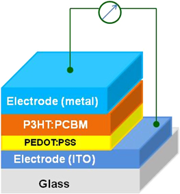
Figure 1. A schematic pattern of the organic solar cell nanostructure.
Download figure:
Standard image High-resolution imageWhen AgNSPs are embedded into the spacer, as the incident angle increases, both the spectral and total enhancement factors increase, independent of the NSP's size and spacing. The fundamental physics is that the near-field energy of a metal NP is mainly distributed along the polarization direction of the incident E-field, which is critically different from the far-field scattering, where the energy scatters to the propagation direction of the incident light. On the contrary, the NSPs embedded into the active layer offer stronger optical absorption. The scattering energy from the NSPs is directly and sufficiently absorbed by the continuous active material, uncorrelated with the directional property of the electrical near field. Owing to the plasmon coupling and hybridization, the close-packed NSPs have more concentrated near-field distribution, leading to layer enhancement.
In order to improve the technique for trapping the Sunlight into the OSC, Choy el al [28] proposed to utilize both a grating organic active layer and grating plasmonic metallic anode in this device, the grating organic active layer being prepared by patterning, while the grating plasmonic metallic anode being fabricated by a nanoimprint method. As a concrete example of an OSC the authors chose the device with the following structure: ITO/TiO2/active layer/MoO3/Ag organic material of active layer being the polymer blend P3HT:PCBM. With this nanostructure both the SPP and diffraction effects can be explored to improve LT as well as PCE. The performances of OSCs were investigated when the anode is Ag without grating (first case) or is Ag with grating (second case).
The authors obtained the following experimental results. With the grating PCE of the devices increased from 3.09% to 3.68%, this improvement of PCE was attributed to that of current density–voltage (J–V) characteristics Jsc from 8.34–9.03 mA cm−2 and the increase of the FF from 0.580–0.635. Besides, the series resistance of the devices decreased from 9.8 Ω cm2 to 8.1 Ω cm2. For understanding the origin of the Jsc increment, the authors measured also the incident photon to electron conversion efficiency (IPCE) spectra of the devices. It was shown that IPCE increased over the whole wavelength range, particularly in the region of 380–550 nm. Moreover, there was a significant enhancement around ∼715 nm where P3HT did not absorb strongly. The reflection spectra of both patterned and nanopatterned devices at normal incidence were measured. It was observed that the reflectance of the patterned device was reduced over a wide range from ∼400 to 800 nm, large decreases in reflectance having been observed at ∼420 nm and ∼715 nm after fabricating the grating on the device. These decreases in reflectance corresponded to improved absorption in the active layer. To further clarify the data, the authors calculated the ratio between the IPCE of devices with and without grating and observed distinct peaks at ∼400 nm and ∼715 nm where reflectance drastically decreased. To elucidate physical origins of these absorption peaks the author rigorously solved Maxell equations governing optical properties of polymer solar cell by using FDTD method [27] and achieved the agreement of experimental data with theoretical calculations.
Thus the authors have demonstrated that the nanograting array greatly enhanced the light absorption through light diffraction and surface plasmon polarization modes. As a consequence, beside offering the physical mechanisms of the optical enhancement this work demonstrated an effective method to improve light harvesting in polymer solar cells: adopt directly patterned active layer, perform Ag grating and appropriately design the structure. Although the authors used a particular inverted polymer solar cell as a concrete example for clearly explaining the principles, the elaborated method could be applied to improve light harvesting in other types of solar cells.
With the purpose to fabricate the efficient inverted polymer solar cells with directly patterned active layer and silver back grating Choy et al [29] investigated the effects of a directly patterned active layer together with silver nanograting arrays as the anode of inverted polymer solar cells (PSCs). Devices with structure of ITO/TiO2/active layer/MoO3/Ag (with or without grating) were fabricated by using the nanoimprint method. Subsequently, polymer solution of poly(3-hexylthiophene) (P3HT): [6, 6]-phenyl-C61-butyric acid methyl ester (PBM) in chlorobenzene was spin-coated on top of the TiO2 layer. The active layer thickness is about 100 nm.
The morphology of the sample was characterized using atomic force microscopy (AFM) in tapping mode and scanning electron microscopy (SEM). The reflection spectra were experimentally determined by using an ellipsometer. The current density–voltage (J–V) characteristics and incident photon to electron conversion efficiency were measured by standard methods.
To theoretically investigate the optical properties of the PSC the authors employed the finite-difference frequency-domain (FDFD) method. Complex couplings or hybridizations between surface plasmon polariton (SPP) and Bloch modes supported in the metallic grating nanostructure were fully taken into account. The near-field distribution and absorption enhancement factor of PCSs with the metallic grating were obtained by the FDFD method.
The performance of PSCs with the structure ITO/TiO2/P3HT: PCBM/ MoO3/Ag without (control device) and with grating was investigated. The current J-V characteristics were recorded. It was shown that the PCE of the device with grating improved from 3.09% (control device) to 3.68% (grating device). PCE improvement was attributed to that of short-circuit current density (Jsc) from 8.34–9.03 mA cm−2 and FF improvement from 0.580–0.635. The higher FF is a consequence of the nanoimprinted pattern increasing the interface area. Besides, the series resistance of the device decreasing from 9.8 Ω cm−2 (without grating) to 8.1 Ω cm−2 (with grating) is also a cause for a higher FF.
This work clarified the physical origin of plasmonic band edge resonance and its role in enhancing the optical absorption of PSC. As a consequence, besides offering the detailed physics of the optical enhancement, this study demonstrated an effective and simple approach (through adopting a directly patterned active layer to form Ag gratings and appropriate design of layer material and structures) to improve light harvesting of an inverted structure for practical use.
The optical and electrical properties of OSCs incorporating two-dimensional periodic metallic back grating as an anode were also theoretically investigated. The authors developed a model for plasmonic OSCs by solving Maxwell equations and differential equations for the physical quantities of the semiconductor (Poisson, continuity, and drift-diffusion equations). The unified finite-difference approach was adopted to model both the optical and electrical properties of OSCs. For typical active polymer materials, low hole mobility, which is about one magnitude smaller than electron mobility, dominates the electrical property of OSCs. Since the surface plasmon resonances excited by the metallic grating produced concentrated near-field penetration into the active polymer layer and decayed exponentially away from the metal-polymer interface, a significantly nonuniform and extremely high exciton generation rate took place near the grating. The authors found that the reduced recombination loss and the increased open-circuit voltage can be achieved in plasmonic OSCs. The blend active layer of the OSC was chosen to be P3HT: PCBM. The cathode and anode of the OSC comprised the transparent and conductive material TiO2 and the Ag-PEDOT:PSS-Ag (lateral) grating layer, respectively. The standard cell, which replaced the Ag-PEDOT:PSS flat layer, was also modeled. The authors obtained the following values of the characteristic parameters of plasmonic and standard OSCs:
- -Short-circuit current Jsc = 62.84 A m−2 for plasmonic OSC and 41.67 A m−2 for standard OSC,
- -Open-circuit voltage Voc = 0.62 V for plasmonic OSC and 0.61 V for standard OSC,
- -Fill factor FF = 0.55 for both plasmonic and standard OSCs,
- -Power conversion efficiency PCE = 2.15% for plasmonic OSC and 1.4% for standard OSC.
In a subsequent work [30] Choy et al again proposed and experimentally demonstrated new dual metallic nanostructures composed of AuNPs (for the LSPR) embedded in the active layer and a Ag nanograting electrode (for the SPP) as the back reflector in inverted OSCs. Through the collective excitation of Floquet modes, SPPs, LSPRs, and their hybridizations, the authors achieved simultaneously both the broadband absorption enhancement and positive electrical effects. For designing new dual plasmonic OSCs the authors have clarified the fundamental physics of various optical phenomena as well as the role of metallic nanostructures in improving the optical and electrical properties of OSCs. They have also demonstrated the accumulated electrical and optical improvements that can realize considerable absorption enhancement and achieve an 8.79% PCE in inverted OSCs.
The current density–voltage (J–V) characteristics and photovoltaic parameters of different structural devices were experimentally determined. For understanding the physical mechanisms of PCE improvement the authors first optimized the device performance with one type of metallic nanostructure (i.e., AuNPs only or Ag nanograting only) then investigated the effects of a dual metallic nanostructure (i.e., both AgNPs and Ag nanograting in one single device) on the PCE improvement.
In brief, in this work the dual metallic nanostructures were demonstrated in single OSCs by simultaneously incorporating AuNPs into the active layer and fabricating the Ag nanograting electrode by means of a newly proposed room-temperature, vacuum-assisted nanoimprint method.
Apart from the waveguide modes and diffraction, the authors simultaneously introduced hybridized LSPRs (from AuNPs) and SPPs (from the Ag nanograting) to successfully achieve a broadband absorption enhancement. The detailed mechanisms were described by theoretical studies. As a consequence, the PCE was improved to the very high value 8.79%.
With the interest in using a multiple-grating structure to improve the technique for trapping the Sunlight into thin-film solar cells, Abass et al [31] proposed to use triangular dual-interface grating (DIG) structures and performed a numerical study of complex triangular DIG systems to enhance the absorption efficiency of thin-film solar cells. The front grating (at the air side) should ensure that a large proportion of incoming light entered the solar cells. For this purpose the authors followed a gradually varying effective index approach by using triangles in the ITO contact. For the metal back grating the authors also used the triangular geometry enhancement with the ITO grating occurring at shorter wavelengths (<720 nm) and via a resonance peak due to (dielectric) waveguide made excitation around 880 nm. The main mechanism for the enhancement at shorter wavelengths was due to the scattering by ITO triangle features. For the structure with only Ag back contact, the main enhancement occurred at longer wavelengths (>750 nm) due to the excitation of a waveguide mode at 780 nm and a plasmonic mode at 838 nm. The combined grating structure led to a better overall enhancement. The authors obtained an integrated absorption of the AM 1.5 G spectrum in the 400–950 nm wavelength region of 83.10% for the DIG structure and 71.96% for the flat one.
For LT with a high efficiency, it is desirable that the incoming broadband radiation couples to as many waveguide and SPP modes in solar cells as possible. To achieve this purpose the authors proposed to use the multiperiodic as well as the blazed DIG structures. Detailed calculations of these complex structures were also carried out.
In reference [32] Kalfagiannis et al investigated the performance of OSCs with the incorporation of AgNPs into the device at two distinct places: AgNPs were deposited either on the top of the ITO transparent anode prior to the deposition of the PEDOT:PSS layer separating the ITO transparent electrode and the P3HT: PCBM active layer prior to the deposition of the cathode or on the top of the active photovoltaic layer (figure 2). Optical properties of individual layers as well as of the device were determined by spectroscopic ellipsometry (SE) as well as by variable angle reflectance and scattering spectroscopies. These optical methods were used to quantify the plasmonic effect of the devices doped with the AgNPs in correlation with the device electrical characteristics, measured both in the dark and under illumination. SE results showed enhanced absorption in the visible spectral range for both configurations, but it was more pronounced in the case where AgNPs were in direct contact with the active layer. Moreover, placing AgNPs on the top of the ITO transparent anode resulted in better overall performance of the device.
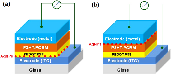
Figure 2. Schematic of organic solar cell with AgNPs on top of (a) indium tin oxide (ITO) and (b) the active layer (P3HT:PCBM).
Download figure:
Standard image High-resolution imageHigh-performance polymer solar cells employing the plasmonic effect of multi-positional silica-coated silver NPs (Ag@SiO2) were demonstrated by Park, Kim et al [33]. The silica shell in Ag@SiO2 preserved the LSPR effect of AgNPs by preventing oxidation of the Ag core under ambient conditions and also eliminated the concern about exciton quenching by avoiding direct contact between the Ag core and the active layer. The multipositional property referred to the ability of Ag@SiO2 NPs to be introduced at both ITO/PEDOT:PSS (type I) and PEDOT:PSS/active layer (type II) interfaces in polymer solar cells due to the silica shell.
Prepared AgNPs were spherical and had uniform diameters of about 50 nm. The silica shell uniformly and completely coated the surfaces of individual AgNPs with an average thickness of 10 nm. Uniform films of Ag@SiO2 NPs were formed on silicon substrates via spin coating. The UV–Vis absorption spectrum of the Ag@SiO2 solution dispersed in ethanol was measured. Compared to that of bare NPs with the same size of about 50 nm, the Ag@SiO2 spectrum exhibited a red-shifted LSPR peak at 450 nm, the red shift being caused by the silica shell.
Two types of solar cells with the following structures were fabricated: type I: ITO/Ag@SiO2/PEDOT:PSS/PTB7:PCBM/Al; type II: ITO/PEDOT:PSS/Ag@SiO2/PTB7:PCBM/Al. Reflectance measurements were carried out to elucidate total light absorption spectra of both types of fabricated solar cells as well as that of the solar cell without Ag@SiO2 used as the reference. Other physical characteristics such as short-circuit current density (Jsc), open-circuit voltage (Voc), FF, PCE, and EQE of both types of solar cells as well as of the reference one were determined from the experimental data. The authors obtained fthe ollowing results for Jsc, Voc, FF, PCE, and EQE (table 1).
Table 1. Physical parameters of solar cells type I and type II.
|
Jsc (mA cm−2) | Voc (V) | FF | PCE (%) | EQE (%) |
|---|---|---|---|---|---|
| Reference | 14.64 ± 0.14 | 0.74 ± 0.1 | 0.67 ± 0.01 | 7.51 | 69.4 |
| Type I | 16.10 ± 0.21 | 0.74 ± 0.1 | 0.67 ± 0.01 | 8.20 | 77.3 |
| Type II | 16.65 ± 0.12 | 0.74 ± 0.2 | 0.68 ± 0.02 | 8.92 | 81.3 |
Thus the authors firmly demonstrated that the incorporation of Ag@SiO2 NPs into the PTB7: PCBM-based polymer solar cells remarkably improved device performance in both type I and II structures.
It was well known that for improving the performance of thin-film solar cells there were two different approaches: either to form a photonic nanostructure on the transparent electrodes, such as fluorine-doped tin oxide (FTO), or to utilize the plasmonic enhancement effect of AuNPs deposited on the surface of the device. In reference [34] Wu et al explored the combination of both above-mentioned approaches to achieve the integrated efficiency of the LT. The advantage of implementing the combined plasmonic–photonic nanostructures on electrodes instead of inside the semiconductors is to minimize generating additional defects as charge traps that reduce charge mobility and increase charge recombination. Measurements of light scattering and plasmonic effects on these samples in comparison with those on the photonic nanostructured FTO allow comparison of the combined effects of plasmonic–photonic nanostructures on FTO with separated effects of plasmonic and photonic counterparts.
The plasmonic–photonic nanostructured FTO electrode was fabricated according to the following procedure. At the beginning a nanopatterned FTO electrode was fabricated using nanoimprint lithography, followed by reactive ion etching. Then AuNPs with lateral dimensions around 100 nm were deposited on a patterned FTO electrode by the e-beam evaporation method, followed by thermal annealing to form the plasmonic–photonic nanostructure on FTO.
Scanning electron microscopy (SEM) was applied to analyze the surface morphology of the samples. It was shown that at a high annealing temperature of 550 °C most of the Au particles were rounded with diameters of 50–200 nm. Optical transmittance spectra of three AuNP-deposited flat FTO samples were recorded. Two of them were annealed at 550 °C, while the third one was not annealed.
The LSPR of the first two samples was clearly seen at ∼580 nm, but the LSPR wavelength was much longer, at ∼750 nm. It is worth noting that the sample annealed at 550 °C exhibited a stronger LSPR than that annealed at 300 °C, which may be ascribed to differences in the AuNPs' shape. At a higher annealing temperature, AuNPs are more rounded and collapse onto the substrate, resulting in better contact with the substrate with a hemisphere shape and slightly increased particle size.
To obtain some insights into the origin of the LSPR features on the observed transmission curves, the authors carried out the FDTD simulation. A gold NP with a disk shape was placed at the interface between FTO and air, and a plane light wave was normally launched with a single polarized electric field Ex. Perfectly matched layer conduction was assumed for the boundary of the simulation window, which absorbs the energy without inducing reflections. The transmittance was evaluated by placing a power meter 30 nm away from the Au/FTO interface inside the FTO film to measure the optical power that passed through the interface. The measured power was then normalized for the case of with or without AuNPs on the interface. The Drude model was applied for the complex dielectric function of Au. On the basis of the Mie scattering theory, plasmonic resonance wavelength is determined by both the material property and the size of the metal particle, as well as the dielectric constant of the medium surrounding the metal particle. Assuming that the particle size is much smaller than the wavelength, the classical formula for Rayleigh scattering can be used, and the scattering cross section is proportional to
where λ is the wavelength, a is the radius of the particle, and εp and εm are the dielectric function of the metal and the dielectric constant of the medium. Because the real part of the dielectric function εp is negative, and its magnitude increases with the wavelength, the resonance of scattering cross section in the vicinity of Reεp = −2εm would move to a longer wavelength with the increase of εm. The inlaid AuNPs have better contact with the substrate and hence a stronger dielectric effect on the substrate, which contributes to increased resonance absorption as well as the red shift of the resonance wavelength.
A new method to enhance LT into polymer cells by doping plasmonic metallic NPs into dual charge-selecting interfacial layers was proposed and realized by Chen, Jen et al [35]. The authors employed the bis-adduct fullerene surfactant (C70-bis), which was also used in several earlier works on polymer solar cells [36–39]. They prepared AuNPs with three different sizes of 20, 50, and 70 nm, measured the absorption spectra of these AuNPs in water, and observed the plasmon resonance peaks at 521, 530, and 544 nm, respectively, in good agreement with the theoretical calculation. Note that the plasmon resonance peak of AuNPs red-shifted with the increasing size.
Due to different dielectric permittivities, the plasmon resonance peaks of these AuNPs also red-shifted for each size of AuNP in PEDOT:PSS and in C70-bis, with peaks red-shifted more in C70-bis than in PEDOT:PSS.
At the beginning the performance of polymer solar cells with AuNPs doped in the rear interfacial layer was investigated. The J–V curve of the device with optimal doping condition (50 nm, 0.5 wt%) exhibited the following characteristics: Jsc = 12.24 mA cm−2, Voc = 0.87 V, PCE =6.99%, FF = 0.65; while those of the reference one were: Jsc = 11.69 mA cm−2, Voc = 0.87 V, PCE = 6.65%, FF =0.65. Then the authors investigated the performance of the polymer solar cell with AuNPs doped in both interfacial layers at the optimal doping conditions (50 nm and 0.5 wt% AuNPs at the rear side and 70 nm and 0.5 wt% at the front side). The following characteristics were obtained: Jsc =12.90 mA cm−2, Voc = 0.87 V, PCE = 7.5%, FF = 0.67.
Devices with AuNPs doped only in the front interfacial layer were also investigated. It was shown that Jsc in the devices with AuNPs doped in both interfacial layers were enhanced more than either of those with AuNPs doped only in one interfacial layer.
In brief, the authors successfully performed the enhancement of PCE of polymer solar cells with dual charge-selecting interfacial layers on both rear and front sides to enhance LT into the devices.
Mono-dispersive metallic NPs possess a single resonance peak. Therefore the PCE of OSCs doped by mono-dispersive metallic NPs can be enhanced only in a narrow spectral region. To enhance the overall efficiency of OSCs Choy et al [40] proposed to use the shape-dependent broadband plasmonic absorption of metallic NPs with different shapes by combining Ag (spherical) NPs and Ag nanoprisms. The diameter of AgNPs was about 20 nm, while the side lengths were around 60 and 10 nm, respectively. The absorption spectra of these nanomaterials dispersed in water were measured. Ag (spherical) NPs and Ag nanoprisms had maximum absorption peaks around 400 nm and 600 nm, respectively, which arose from the LSPRs of two materials with two different shapes. After mixing these two types of materials, a broader absorption covering the 400–600 nm range was obtained.
For demonstrating the plasmonic effect of prepared metallic nanomaterials on the optical absorption of the devices, the author investigated the incident photon-to-electron conversion efficiency (IPCE) with respect to the monochromatic light, compared the JSC values from the J–V characteristic with those calculated from IPCE data with the AM1.5G reference spectrum and obtained a rather good agreement (within 4%). As a result, the Jsc values of the control, the devices with spherical AgNPs only as well as with Ag nanoprisms only with mixed metallic nanomaterial consisting of both spherical AgNPs and Ag nanoprisms, were 8.65, 9.57, 9.63, and 10.42 mA cm−2. Thus a broadband absorption of OSCs was realized by combining differently shaped nanostructures exhibiting varied LSPRs and regions of scattering into the active layer. For the Ag nanomaterial-doped OSCs, the enhancement of the JSC value in the cases of spherical AgNPs, Ag nanoprisms, and blended Ag nanostructure was approximately 9.0%, 10.1%, and 17.91%, respectively, compared to the control. As a result, the OSCs with mixed Ag nanostructures exhibited a high efficiency, with a PCE of 4.3%.
A comprehensive study on ultrathin, highly efficient broadband OSCs enhanced by a plasmonic cavity with a sub-wavelength hole array (PlaCSH) was performed by Chou and Ding [41]. Each device consisted of a thin metal-mesh electrode with sub-wavelength hole array (MESH), an active semi-conductivity layer (A), and a metal sheet (M); i.e., it had the structure MESH/A/M. The authors focused on the effect of the PlaCSH structure rather than the effects of the polymer materials, compositions, and processing conditions and used P3HT/ PCBM as an example. All features of MESH (i.e., the pitch, hole size, and hole separation) were sub-wavelength. The back electrode was a good metallic light reflector. The PlaCSH was designed such that a significant portion of incoming light was transmitted through the MESH into the cavity, and then most of the transmitted light was trapped and absorbed by the cavity. The authors achieved a total light absorption (lumped effect of transmission, trapping, and absorption) as high as 96% and broad bandwidth (e.g., nearly constant from 400–900 nm) and observed that the PlaCSH can also reduce the light reflection and absorption by MESH by two- to six-fold compared to that when the MESH was alone.
Compared to solar cells with an ITO electrode, PlaCSH enhanced the PCE, Jsc, and FF of OSCs by 52%, 41%, and 6%, respectively. The EQE enhancement factor, defined as the ratio of EQEs of PlasCSH to ITO solar cells, was as high as 133% at 550 nm and 220% at 650 nm. For understanding the origin of the enhancement of PlaCSH solar cells compared to conventional ones, the authors provided a detailed study on physical mechanisms of various enhancement effects, such as the perfect light coupling and trapping in PlasCSH solar cells and the broad bandwidths, as well as broadband and Omni acceptance leading to high absorption and low reflection in PlaCSH solar cells. They also measured the electrical and optical characteristics of MESH on glass, compared MESH optical characteristics before and after PlaCSH solar cell formation, considered the effect of PlaCSH cavity length, and performed the optimization of PlaCSH solar cells.
The benefits of using various plasmonic nanostructures for broadband, polarized-independent, and angle-insensitive absorption enhancement, as well as their integration in solar cells, were discussed by Gan et al [42]. The authors presented a review of the research on plasmonic-enhanced solar cells with the potential of significantly increasing the PCE beyond the 10% barrier. The discussed scientific topics included the following issues:
- (a) Metallic nanoparticles
Metallic NPs were the most popular, simplest, and extensively employed nanostructures for enhancing the performance of solar cells due to the plasmonic effect. They were deposited (doped) in the devices either outside or inside the active layer(s) and either randomly distributed or formed ordered symmetric arrays.
- (b) Symmetric plasmonic nanostructures
Both one- (1D) and two-dimensional (2D) periodic nanostructures were explored to achieve certain features of OSCs. Due to the polarization dependence of the 1D grating nanostructures, the LT behavior for TE and TM modes were usually very different: only the TM mode with the magnetic field parallel to the 1D nanogratings contributed to the SPP mode. This strong polarization dependence could be beneficial for particular application like polarized absorption filters for energy recycling in color-display applications. In the case of 2D periodic metallic nanostructures, the incident light with various polarization components could be coupled to SPP modes in different directions along the metallic interface, leading to a polarization-insensitive response beneficial to increasing sunlight absorption.
- (c) Broadband absorption enhancement
Broadband absorption enhancement is needed over the entire visible and part of the near-infrared solar spectrum in order to improve the efficiency of solar cells. For thin metal films with a thickness less than 100 nm, two single SPPs interacted with each other and led to two coupled SPPs, the long-range SPP and short-range SPP. The bandwidth of the short-range SPP was much broader than the other two SPP modes and was beneficial for broadband absorption enhancement. Introducing a second array of metallic NPs on the other side of the active layer also led to further enhancement in the optical absorption of the active organic layer. Moreover, the distance between two plane nanostructures could be as small as tens of nanometers. In this case they would form a vertical nano-antenna array and support coupled modes within the gap between these two plasmonic nanopatterned layers.
Besides the broadband absorption enhancement, the angle-insensitive, Omni-directional absorption enhancement and the dual use of nanopatterned metallic films as electrodes, as well as for LT in order to achieve simultaneously electrical and optical functionalities, were also discussed.
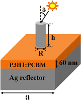
Some time ago Le et al [43, 44] theoretically demonstrated broadband total optical transmission through metallic screens (metascreens) containing narrow 2D apertures. At a specific incident angle, such transmissions resulted in zero reflection over a broad bandwidth, without necessarily relying on SPRs. It was the equivalent of a Brewster transmission in corrugated metascreens, providing total transmission for TM polarization. This finding hinted at perfectly absorbing energy-harvesting devices. It might provide the efficient means of trapping light, with TM polarization over ultrabroad bandwidths. In a subsequent work [45] Le explored using these perforated metascreens as plasmonic resonance antennae. Light could be concentrated to allow LSPR excitation at normal incidence. They employed impedance matching at a specific oblique incidence to improve absorption in thin OSCs over a broad bandwidth and broad angular range. The polymer photovoltaic solar cell had the structure presented in figure 3.
Figure 3. Structure of polymer photovoltaic solar cell with metascreens as plasmonic resonance antennae. (With permission from author [45]).
Download figure:
Standard image High-resolution image
The active layer consisted of the electron donor P3HT and acceptor PCBM. Silver was selected as the backside contact because of its low absorption loss. It also provided strong surface plasmon resonance modes, required for strong field enhancement in the active layer. All simulations were carried out for a solar cell of an active layer thickness of 60 nm and P3HT:PCBM weight ratio of 1:1. Numerous simulations were carried out for various cylindrical antenna dimensions (R, h) and lattice constant (a) to ensure maximum integrated absorption efficiency (AEtot). A maximum AEtot of 58.5% was achieved for the parameters a, R, and h being 300, 45, and 200 nm, respectively. The thin polymer active layer absorbed 58.5% of the AM1.5G spectrum over the 300–800 nm range. This increase of AEtot from 48–58.5% for flat and 2D array antenna-containing cells, respectively, represented 22% enhancement. The integrated light absorption and optical properties of the device were the same for all polarizations at normal incidence.
Thus 2D arrays of Ag cylindrical antennae integrated on thin-film OSCs resulted in an absorption enhancement of up to 22%. They enabled the broadband absorption of sunlight for TE- and TM-polarizations over a wide incident angle range.
A simple method using 40 nm AuNPs with various concentrations to improve PCE in BHJ polymer solar cells based on blended P3HT:PCBM was demonstrated by Zhang et al [46]. The AuNPs were deposited on IT) substrates by spin coating from colloidal solution prior to deposition of a PEDOT:PSS buffer layer. It has been found that both short-circuit current density and PCE increased after incorporating AuNPs between ITO and the PEDOT:PSS layer, and with a suitable density of Au NPs the maximum enhancement of device efficiency was achieved: The PCE increased from 3.50–3.81%, corresponding to a 9% enhancement, when the BHJ solar cells were incorporated with 0.9 wt.% AuNPs.
Surface morphologies of AuNPs and the subsequent layers were characterized by AFM and SEM. The UV–Vis absorption spectra of films on ITO and silica substrates were recorded with a UV–Vis spectrophotometer in double-beam mode. The EQE was measured using a lock-in amplifier with a current preamplifier under short-circuit conditions after illuminating the cells with a monochromator. The current–voltage characterizations of the device with the 0.9 wt.% AuNPs and of the reference device were recorded. The reference device exhibited an open-circuit voltage (Voc) of 0.648 V, a short-circuit current density (Jsc) of 9.37 mA cm−2, and an FF of 0.577, resulting in a total PCE of 3.50%. After incorporating AuNPs between ITO and the PEDOT:PSS layer, all the devices exhibited a higher Jsc. Especially, the device prepared with the 0.9 wt.% AuNPs exhibited the highest Jsc of 10.35 mA cm2, while the Voc and FF were similar to those of the reference device, and finally a PCE of 3.81% was obtained.
3. Conclusion and discussion
During about two years since the publication of the encouraging work of Atwater and Polman [14], the research on the application of the plasmonic enhancement effect to improve the technique of LT into polymer solar cells has achieved promising results. In the experimental as well as theoretical works on this topic, the following basic elements were employed:
- -AR coating;
- -Randomly distributed on symmetric periodic monolayers of metallic spherical NPs, metallic NPs with different shapes, spherical NPs with core–shell structure, nanovoids;
- -Plasmonic metallic grating;
- -Grating organic active layer;
- -Grating ITO layer;
- -Dielectric grating;
- -Photonic structure;
- -Plasmonic cavity with subwavelength hole array (PlaCSH).
Besides the use of a single element in each plasmonic nanostructure, there were successful attempts to improve LT into polymer solar cells by simultaneously using two basic elements, such as plasmonic metallic grating and AR coating, plasmonic back and front metallic gratings, PC (dielectric) and plasmonic metallic grating, two plasmonic metallic gratings, plasmonic metallic grating and grating organic active layer, ITO front grating and plasmonic metallic back grating, a multipositional monolayer of spherical NPs with a core–shell structure, combined with a plasmonic–photonic structure, a plasmonic cavity with a PlaCSH. A comprehensive review of the study on using networks of plasmonic metallic NPs was presented in reference [42].
In addition to the research on LT into polymer solar cells, recently methods to improve LT into solar cells of other types were also proposed. For example, Polman and Atwater et al [47, 48] used electromagnetic modeling to study plasmonic enhancement of LT into amorphous Si solar cells, Akimov and Koh [49] designed the plasmonic metallic structure for efficient subwavelength LT in thin-film amorphous Si solar cells, Wang et al [50] applied the simulation calculation to the study of a metamaterial–plasmonic absorbing structure for high efficiency thin-film amorphous Si solar cells, Atwater and Polman et al [51] designed the plasmonic LT in thin-film Si solar cells by coupling antireflection coating with waveguide modes, and Kholmicheva et al [52] developed plasmonic solar cells using a PbS semiconductor nanocrystal. The research on plasmonic enhancement of dye-sensitized solar cells was also initiated [53–61]. We do hope that the present review article will motivate the research on this interesting topic.
Acknowledgments
The authors would like to express their sincere thanks to the Academy of Science and Technology for their support.