

Abstract
In this work the sensitivity of process parameters like channel length (L), channel thickness (tSi), and gate work function (φM) on various performance metrics of an undoped cylindrical gate all around (GAA) metal-oxide-semiconductor field effect transistor (MOSFET) are systematically analyzed. Undoped GAA MOSFET is a radical invention as it introduces a new direction for transistor scaling. In conventional MOSFET, generally the channel doping concentration is very high to provide high on-state current, but in contrary it causes random dopant fluctuation and threshold voltage variation. So, the undoped nature of GAA MOSFET solves the above complications. Hence, we have analyzed the electrical characteristics as well as the analog/RF performances of undoped GAA MOSFET through Sentaurus device simulator.
Export citation and abstract BibTeX RIS

Original content from this work may be used under the terms of the Creative Commons Attribution 3.0 licence. Any further distribution of this work must maintain attribution to the author(s) and the title of the work, journal citation and DOI.
1. Introduction
To achieve low cost, high operational speed and better performance, the dimensions of conventional transistors need to be downscaled to the sub-nanometer region. The reduction of metal-oxide-semiconductor field effect transistor (MOSFET) dimensions will degrade the gate control over the channel due to close proximity between source and drain. This leads to increase various short channel effects (SCEs) such as hot carrier effect, threshold voltage roll-off, and substrate bias effect [1, 2]. Many new devices have been introduced beyond Moore's era [3–5] to suppress the SCEs and enable further scaling down of the device. Similarly, a number of multi-gate silicon on insulator (SOI) technologies have also been proposed to replace the conventional MOSFET [6, 7]. However, the cylindrical gate all around (GAA) MOSFET is one of the novel devices which further enables scaling without hindering the device performance. Because of the low characteristic length and higher drive current, GAA MOSFETs can achieve higher packing density as compared to double gate (DG) MOSFETs [8–10]. Also GAA MOSFET has excellent electrostatic control of the channel, robustness against SCEs, better scaling options, no floating body effect, larger equivalent number of gates, and ideal subthreshold swing as compared to other multiple gate MOSFETs. Hence, the GAA MOSFET is a promising solution for nanoscale technology complementary metal–oxide–semiconductor (CMOS) devices [11–15]. Recently, MOS devices with sub-50 nm channel length demonstrate more than 100 GHz of cut-off frequency [16–18]. Important device parameters such as threshold voltage (Vth), on-off ratio (Ion/Ioff), and cut-off frequency (fT) are very much sensitive to the device geometry such as channel length (L), channel thickness (tSi), and gate work function (φM). In this work an attempt was taken to present a detailed analysis of the performance dependency of GAA MOSFET on device geometry variation.
In this paper, different performance metrics like drain current (ID), transconductance (gm), total gate capacitance (Cgg) and cut-off frequency (fT) are systematically presented with the variation of Lg, φM, and tSi. Along with the introduction, section 2 describes the device structure description that includes all the dimensions, materials and doping concentrations of GAA MOSFET. This section also analyses the physics of the device using device numerical simulations and models activated for simulation. Section 3 comprises all results and discussion. Finally, the concluding remarks are presented in section 4.
2. Device structure and simulation setup
The schematic diagram of the fully depleted cylindrical GAA MOSFET structure used for modeling and simulation is shown in figure 1. The radial and lateral directions of the channel are assumed to be along the radius and the z-axis of the cylinder as shown in figure 1. The source and drain of the device are uniformly doped with doping concentration of ND = 1 × 1020 cm−3. The channel is kept undoped. The gate oxide thickness is tox = 1.1 nm.

Figure 1. Schematic structure of cylindrical gate all around MOSFET.
Download figure:
Standard image High-resolution imageThe simulation is carried out by the device simulator Sentaurus, a 3D numerical simulator from Synopsis Inc. [19]. To obtain accurate results for MOSFET simulation we need to account for the mobility degradation that occurs inside inversion layers. The drift-diffusion model is the default carrier transport model in Sentaurus device is activated. For the drift-diffusion model, the current densities for electrons and holes are given by
where Jn and Jp are electron and hole current density, μn and μp represent electron and hole mobility, n and p describe electron and hole density, γn and γp are Fermi statistics constants, and mn and mp present spatial effective masses of electron and hole, respectively. T and k describe temperature and Boltzmann constant. EC and EV are conduction and valance energy bands. Dn and Dp represent the diffusion constants for electron and holes respectively.
The first term takes into account the contribution due to the spatial variations of the electrostatic potential, the electron affinity, and the band gap [20, 21]. The remaining terms take into account the contribution due to the gradient of concentration, and the spatial variation of the effective masses mn and mp. All other terms used have their commonplace meanings. In the simulation, basic mobility model is used that takes into account the effect of doping dependence, high-field saturation (velocity saturation), and transverse field dependence. The silicon band gap narrowing model that determines the intrinsic carrier concentration is activated.
3. Results and discussion
In order to analyse the impact of channel length (Lg), and channel thickness (tSi), and gate work function (φM) on the device performance, the simulation is carried out by varying the above parameters. Figures 2(a) and (b) show the drain current (ID) in log scale as a function of gate to source voltage (VGS) for different Lg and tSi, respectively. The GAA MOSFETs are showing a significant low leakage current in the range of 10−12 to 10−14 A μm−1 for all cases. In figure 2(a), Lg varies from 28 to 70 nm and we can observe from the figure that a decrease in Lg results a shift in the characteristics. The off-state current (Ioff) increases dramatically as Lg decreases to below 30 nm with comparison to others. In the short channel device the Ioff increases due to random motion of charge carriers. As channel length decreases, it gives rise to high drain current because of the relation ID ∝ 1/L. However, from the log scale, the leakage current is also prominent for lower channel lengths. Figure 2(b) reveals the ID dependency on silicon body thickness of the GAA MOSFET. The characteristic of Ioff is also influenced by tSi, which is cleared from figure 2(b). As the silicon film gets thinner, there is a significant improvement in leakage current because no further leakage path is available far from the gate.

Figure 2. Drain current (ID) in log scale as a function of gate to source voltage (VGS) for VDS = 50 mV (a) with variation in Lg (b) with variation in tSi.
Download figure:
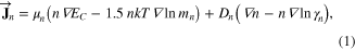
Standard image High-resolution imageFigure 3(a) represents the ID-VGS characteristic for different values of metal gate work function (φM). The work function is varied from 4.6 eV to 5.1 eV for VDS = 50 mV (sub-threshold region of operation). The results illustrate that the off-state leakage current (subthreshold performance) of the device improves for higher values of metal gate work function. This is because the higher φM consequently depicts higher threshold voltage, which further reduces the off-state leakage current and improves the subthreshold behavior of the device. Figure 3(b) shows the intrinsic capacitances (gate to gate capacitance Cgg) as a function of ID for subthreshold or weak inversion with variation in channel length. As shown in figure, the intrinsic capacitance increases with increase in ID. This is because of the increase in the fringing field lines emanating from the gate edges. The device with Lg = 28 nm shows low value for Cgg and as Lg increases the Cgg also starts increasing and obtains its maximum at Lg = 70 nm. Hence, in the case of Lg = 28 nm, the intrinsic capacitance value is smallest, which in turn leads to high cutoff frequency.
Figure 3. (a) Drain current (ID) in log scale as a function of gate to source voltage (VGS) for VDS = 50 mV for different φM. (b) Cgg as a function of ID at VDS = 50 mV with variation in Lg.
Download figure:
Standard image High-resolution imageTransconductance (gm) and cut off frequency (fT) as a function of ID are presented in figures 4(a) and (b), respectively. From the figure, it is clear that as the channel length decreases the gm value is increasing because of high drain current. The high gm will further enhance the transconductance generation factor (TGF = gm/ID) which is the requirement for realization of circuits operating at low supply voltage. From figure 4(b), the variations of cut off frequency (fT = gm/2πCgg) can be observed with respect to VGS for different values of channel lengths. Here, the value of fT obtained for the device having low channel length is higher, and gradually decreases as the channel length increases. fT is inversely proportional to the intrinsic capacitance (Cgg). So, the fT value is low due to high capacitance values for higher channel length devices, as discussed in figure 3(b).

Figure 4. (a) gm as a function of ID at VDS = 50 mV with variation in Lg and (b) fT as a function of ID at VDS = 50 mV for different Lg.
Download figure:
Standard image High-resolution image
All the extracted and calculated values of dc as well as analog/RF performances are tabulated in tables 1– 3 with the variation of silicon body thickness (tSi), gate work function (φM), and channel length (Lg) of the GAA MOSFET respectively. Table 1 compares and analyses the sensitivity of tSi on various important parameters such as Ion, Ioff, and Vth. We can effectively control the Vth and SCEs such as off-state leakage current by reducing tSi with a little compromise in on-state current. Hence, people always prefer ultra-thin body (UTB) fully depleted (FD) SOI MOSFET as the body is completely controlled by the gate and there is no leakage path far from the gate. The percentage of improvement in Ioff is 82.53% and 91.33%, while tSi varies from 15 nm to 10 nm and 10 nm to 5 nm, respectively.
Table 1. DC performance measures with tSi variation.
| tSi (nm) | Ion (μA) | Ioff (pA) | Vth (V) |
|---|---|---|---|
| 5 | 1.21 | 0.11 | 0.419 |
| 10 | 3.99 | 1.27 | 0.405 |
| 15 | 8.31 | 7.27 | 0.4 |
| 20 | 11.4 | 9.7 | 0.387 |
Table 2. DC performance analysis with φM variation.
| φM (eV) | Ion (A) | Ioff (A) | Vth (V) |
|---|---|---|---|
| 4.6 | 3.68 × 10⁻⁶ | 2.44 × 10⁻¹² | 0.382 |
| 4.8 | 1.82 × 10⁻⁶ | 3.99 × 10⁻¹⁵ | 0.587 |
| 4.9 | 3.91 × 10⁻⁷ | 1.58 × 10⁻¹⁶ | 0.639 |
| 5.1 | 1.32 × 10⁻⁹ | 2.45 × 10⁻¹⁹ | — |
Table 3. Analysis of different parameters with Lg variation.
| Lg (nm) | Ioff (A) | gm (max) (μS) | Cgg (max) × x10−17 (F) | fT (max) (GHz) |
|---|---|---|---|---|
| 28 | 2.44 × 10⁻¹² | 16.1 | 1.73 | 222 |
| 40 | 1.14 × 10⁻¹³ | 17.6 | 2.51 | 172 |
| 55 | 3.86 × 10⁻¹⁴ | 16.4 | 3.47 | 116 |
| 70 | 2.48 × 10⁻¹⁴ | 15.2 | 4.4 | 83.6 |
Table 2 reports the similar parameters (as in table 1) but with variation in gate work function (φM) for gate length Lg = 28 nm. The φM is one of the main controlling parameters threshold voltage. As we can measure from the table, Vth is increasing with increase in φM, which further controls the subthreshold leakage current. While φM changes from 4.6 eV to 4.9 eV, a significant improvement in Ioff consequently in SCEs can be observed.
Table 3 summarizes the analog/RF figures of merit (FOMs) for different values of channel lengths. It is clear from the table that, while the gate length is reduced, the RF FOM fT is increased because of high drain current which results in higher gm values for shorter gate length devices.
4. Conclusion
A cylindrical gate all around (GAA) MOSFET is explored and the performance evaluation is carried out with extensive device simulation by Sentaurus simulator. The sensitivity of device parameters like tSi, φM, and Lg on various dc and analog/RF FOMs are systematically presented. From our results, by considering an ultra-thin body (UTB) and little higher gate work function can enhance the device performance with well suppressed SCEs. The subthreshold leakage current can be significantly improved for lower tSi and higher φM values. Similarly, continuous miniaturization of Lg is required for obtaining high Ion, gm, and fT. Hence, an appropriate selection of the silicon thickness, and metal gate work function give rise to an optimum threshold voltage at a given channel length and drain bias.