

Abstract
Electroplating is an important step in microfabrication in order to increase thickness of undersized parts up to a few micrometers with a low-cost, fast method that is easy to carry out, especially for metals such as copper, nickel, and silver. This important step promotes the development of the fabrication technology of electronic devices on a flexible substrate, also known as flexible electronic devices. Nevertheless, this technology has some disadvantages such as low surface uniformity and high resistivity. In this paper, parameters of copper electroplating were studied, such as the ratio of copper (II) sulfate (CuSO4) concentration to sulfuric acid (H2SO4) concentration and electroplating current density, in order to obtain low resistivity and high surface uniformity of the copper layer. Samples were characterized by scanning electron microscopy (SEM), four-point probe, and surface profiler. The results showed that the sample resistivity could be controlled from about 2.0 to about 3.5 μΩ · cm, and the lowest obtained resistivity was 1.899 μΩ · cm. In addition, surface uniformity of the electroplated copper layer was also acceptable. The thickness of the copper layer was about 10 μm with an error of about 0.5 μm. The most suitable conditions for the electroplating process were CuSO4 concentration of 0.4 mol l−1, H2SO4 concentration of 1.0 mol l−1, and low electroplating current density of 10–20 mA cm−2. All experiments were performed on a flexible polyethylene terephthalate (PET) substrate.
Export citation and abstract BibTeX RIS

Original content from this work may be used under the terms of the Creative Commons Attribution 3.0 licence. Any further distribution of this work must maintain attribution to the author(s) and the title of the work, journal citation and DOI.
1. Introduction
Nowadays, electroplating is an important step in the fabrication process of printed circuit boards (PCBs) and micro-antenna devices [1–3]. Generally, the electroplating step is a process that uses electrical current to reduce dissolved metal cations in order to form a metal coating on a substrate. PCBs and micro-antenna devices are usually made of copper due to its low electrical resistivity (16.78 nΩ · m at 20 °C) and cheap price. This makes the devices to have low resistance and low price.
Recently, there has been a focus in the fabrication technology of electronic devices on reducing the device price by using a flexible substrate such as polyethylene terephthalate (PET) and liquid crystal polymer [3–6]. Beside the advantage of low price, flexible substrates have many other advantages such as non-brittleness, sticking to various object surfaces, and being laminated with an adhesive layer easily [3, 4]. However, the problem with a flexible substrate is the adhesion of the copper layer on it. In order to solve this problem, researchers use a copper thin film deposited by a sputtering method, such as a seeding layer [2, 7]. The seeding layer is subsequently thickened by the electroplating method to reduce the device cost. Nevertheless, the electroplating method has its own problems: low surface uniformity and unstable resistivity. For PCBs, the thickness of the layer must be well controlled, and the electroplating film must have high surface uniformity. For antenna devices, control of resistivity is more important. Therefore, stable resistivity and high surface uniformity are problems that need to be solved in order to fabricate flexible devices with low price and good performance.
In this work we carried out a study on parameters of the electroplating process such as ratio of copper (II) sulfate (CuSO4) concentration to sulfuric acid (H2SO4) concentration and electroplating current density in order to obtain a copper layer on a PET substrate with low resistivity and good surface uniformity.
2. Experimental methods
2.1. Materials
Copper sulfate pentahydrate (CuSO4.5H2O), sulfuric acid (H2SO4), and hydrochloric acid (HCl) were bought from Merck (Germany). Cu-7979, a surface additive, was bought from the MinhChat Company. PET substrates are commercial products; their thicknesses are about 80 μm.
2.2. Experimental setup
2.2.1. Experimental preparation
Firstly, PET substrates were cleaned and used for depositing a thin film of copper using a dc magnetron sputtering Leybold Univex 350 system with the appearance of inert argon (Ar) gas. These parameters were shown in table 1. Almost all samples have the same dimension of 5 × 5 cm2, except samples for Hull cell testing, which have a dimension of 10 × 10 cm2.
Table 1. Parameters of sputtering system.
| Power (W) | Time (min) | Argon (sccm) | Pressure (mbar) |
|---|---|---|---|
| 100 | 15 | 5 | 2.1 × 10⁻³ |
Chemical compositions of four electroplating solutions are shown in table 2. The concentration of sulfate anion, hydrochloric acid, and Cu-7979 were kept invariable in all four solutions. Four electroplating solutions had the ratio of copper (II) sulfate (CuSO4) concentration to sulfuric acid (H2SO4) concentration of 1.33, 0.75, 0.40, and 0.17 and were called 01–1.33, 02 − 0.75, 03 − 0.40, and 04 − 0.17, respectively.
Table 2. Chemical composition of electroplating solutions.

|
01–1.33 | 02–0.75 | 03–0.40 | 04–0.17 |
|---|---|---|---|---|
| Sulfate anion (mol l−1) | 1.4 | |||
| CuSO4 (mol l−1) | 0.8 | 0.6 | 0.4 | 0.2 |
| H2SO4 (mol l−1) | 0.6 | 0.8 | 1.0 | 1.2 |
| CuSO4/H2SO4 | 1.33 | 0.75 | 0.40 | 0.17 |
| HCl (μl l−1) | 137 | |||
| Cu-7979 (ml l−1) | 10 | |||
2.2.2. Hull cell testing
Before electroplating, samples of copper thin film on a PET substrate were dipped in these solutions and were tested by a 267 ml Hull cell bath in order to find the range of suitable current density for each solution. Hull cell testing is considered to be a simple method to control and evaluate various parameters of electroplating processes [8]. The dimensions and top section of the Hull cell bath are shown in figure 1. The current densities along the cathode are shown in following equation [8]

where jc is the cathode current density (mA/cm2), I is the total current electroplating (A), and xc is a coordinate along the cathode (cm).

Figure 1. The dimensions and top section of Hull cell bath.
Download figure:
Standard image High-resolution imageThe result of Hull cell testing with I = 1 A in a solution of 03 − 0.40 is shown in figure 2(a). This result has shown that the copper surface was good when xc was between 1.5–6.5 cm. According to equation (1), the range of suitable electroplating current density was between 8.4–41.8 mA cm−2. However, the experimental result has shown that the electroplating current density of 40 mA cm−2 was not suitable for electronic devices with small scale, due to bad adhesion (figure 2(b)). Therefore, the electroplating current densities that were chosen to investigate for each of the four solutions were 10, 15, 20, and 30 mA cm−2. These current densities were also suitable for three solutions 01–1.33, 02 − 0.75, and 04 − 0.17, due to the results of Hull cell testing of these solutions.
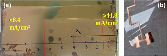
Figure 2. Copper thin film after Hull cell testing in solution of 03 − 0.40 (a), and copper detail with small scale after electroplating with current density of 40 mA cm−2 (b).
Download figure:
Standard image High-resolution image2.2.3. Electroplating experiments
After finding a range of suitable electroplating current densities for four solutions by Hull cell testing, 16 samples of copper thin film on a PET substrate were electroplated in four solutions 01–1.33, 02 − 0.75, 03 − 0.40, and 04 − 0.17, corresponding with four current densities 10, 15, 20, and 30 mA cm−2. All the samples were electroplated with the same electrical quantity of 0.248 A.h. The dimension of the samples is 5 × 5 cm2.
Thicknesses and sheet resistances of samples were measured by a Dektak 6 M surface profiler and a four-point probe from Lucas Labs Division/QuadPro S302-8, respectively. Resistivities of samples were calculated by the following equation [9]

where ρ is the resistivity of sample (Ω m), Rs is the sheet resistance of sample (Ω/▯), and t is the thickness of sample (m). In addition, surfaces of samples were characterized by scanning electron microscopy (SEM) Jeol JSM-6480LV.
3. Results and discussion
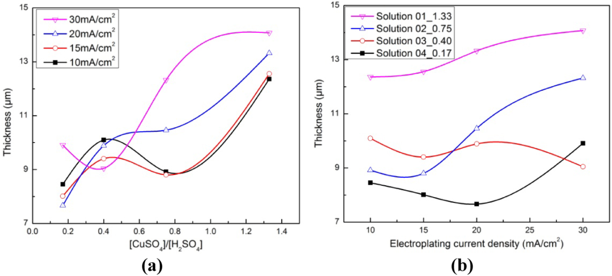
3.1. Samples thicknesses
The thicknesses of samples (μm) are shown in table 3.
Table 3. Thicknesses of electroplated samples (μm) in four solutions 01–1.33, 02 − 0.75, 03 − 0.40, and 04 − 0.17, corresponding to four electroplating current densities 10, 15, 20, and 30 mA cm−2.
| Thicknesses of samples (μm) | ||||
|---|---|---|---|---|

|
01–1.33 | 02 − 0.75 | 03 − 0.40 | 04 − 0.17 |
| 10 | 12.36 ± 0.97 | 8.92 ± 1.24 | 10.10 ± 0.50 | 8.45 ± 0.57 |
| 15 | 12.56 ± 1.22 | 8.80 ± 1.06 | 9.40 ± 0.78 | 8.01 ± 0.62 |
| 20 | 13.32 ± 1.55 | 10.46 ± 1.57 | 9.89 ± 0.97 | 7.67 ± 0.45 |
| 30 | 14.08 ± 1.78 | 12.32 ± 0.78 | 9.05 ± 0.79 | 9.91 ± 1.34 |
All the samples have the same electrical quantity of the electroplating step. According to Faraday's law, which is shown in the following equation, the weight of copper liberated at the anode is proportional to the electrical quantity

where m is weight of material liberated at the anode (g), M is the molar mass of material at the anode, Q is the electrical quantity passed through anode (C), F = 96 485 C mol−1 is the Faraday constant, and z is the valence number of ions of the material at the anode.
All the samples were electroplated with the same electrical quantity so that the mass of copper liberated at the anode in all experiments has the same theoretical value. Nevertheless, the results of the measurement have shown that the thicknesses of samples were not the same (table 3). This can be explained by the difference in electroplating solutions, chemical compositions, and electroplating current densities. Indeed, when the electrons went to cathode, three reactions shown in the following equations could occur in the electroplating process:


Therefore, the appearance of a H+ ion led to some side reactions so that the electroplating efficiency was reduced. The higher the sulfuric acid concentration was, the less efficient it was. Indeed, it is easy to notice the reduction of thickness when the ratio of copper (II) sulfate (CuSO4) concentration to sulfuric acid (H2SO4) was decreased from 1.33 to 0.17 (figure 3(a)).

Figure 3. The influence of the ratio of CuSO4 concentration to H2SO4 concentration (a) and electroplating current density on the thickness of the copper layer after electroplating (b).
Download figure:
Standard image High-resolution imageHowever, the solution with a high concentration of sulfuric acid has the advantage of high surface uniformity. The lowest thickness error was 0.45 μm at solution 04 − 0.17 and a current density of 20 mA cm−2. In addition, thicknesses of samples deposited in solution 03 − 0.40, which have the ratio CuSO4/H2SO4 of 0.40 with various current densities, did not have the large difference (smallest value was 9.05 and largest value was 10.10) (figure 3(b)). This advantage gave this solution an opportunity to be applied to fabricate complicated copper details, which include many edges and polygons. In fact, when complicated copper details were electroplated, the electroplating current density was distributed unevenly: larger at the edge of polygon and smaller at the inside of the polygon. Solution 03 − 0.40, which had a small difference of thickness corresponding with various current densities, could be applied to solve this problem and fabricate complicated electronic details with high surface uniformity.
Thicknesses of the samples were also influenced by electroplating current densities (figure 3(b)). In general, thickness of the sample was increased when current density was increased. Indeed, when the current density increased, the current also increased, and the duration for the electroplating process decreased. It means that the number of electrons which went to cathode per second was higher, and the copper layer was electroplated faster. The faster the electroplating process was, the more pores and defects were formed. This conclusion is verified by SEM images of samples surfaces in figure 4.
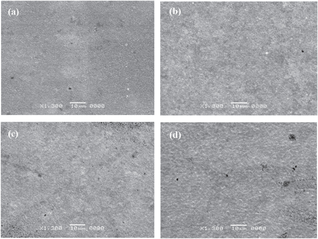
Figure 4. SEM images of samples after copper electroplating in solution 03_0.40 with various electroplating current density: 10 mA cm−2 (a), 15 mA cm−2 (b), 20 mA cm−2 (c), and 30 mA cm−2 (d).
Download figure:
Standard image High-resolution imageThe electroplated surfaces with low current densities got higher surface uniformity and fewer defects than the electroplated surfaces with high current densities. When the sample had many defects, the inside structure became very porous. That is the reason why the sample thickness was increased while increasing the current density.
Electroplating solution 04 − 0.17 with current density of 20 mA cm−2 was the best to obtain a copper layer with high surface uniformity. However, this solution was not suitable to fabricate complicated copper details in reality, because a small difference of current densities could lead to a large difference of thicknesses (figure 3(b)). Therefore, electroplating solution 03 − 0.4 with low current density between 10–20 mA cm−2 was the most suitable electroplating solution in order to form a high surface uniformity copper layer.
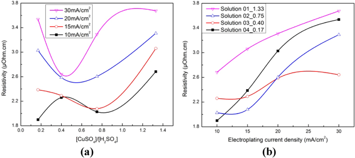
3.2. Sample resistivities
The resistivities of samples (μΩ cm) are shown in table 4.
Table 4. Calculated sample resistivities (μΩ cm) in four solutions 01–1.33, 02 − 0.75, 03 − 0.40, and 04 − 0.17, corresponding to four electroplating current densities 10, 15, 20, and 30 mA cm−2.
| Resistivity (μΩ cm) | ||||
|---|---|---|---|---|

|
01–1.33 | 02 − 0.75 | 03 − 0.40 | 04 − 0.17 |
| 10 | 2.683 ± 0.507 | 2.027 ± 0.698 | 2.260 ± 0.451 | 1.899 ± 0.420 |
| 15 | 3.061 ± 0.637 | 2.078 ± 0.602 | 2.291 ± 0.579 | 2.386 ± 0.566 |
| 20 | 3.309 ± 0.820 | 2.603 ± 0.871 | 2.586 ± 0.662 | 3.028 ± 0.821 |
| 30 | 3.675 ± 0.885 | 3.291 ± 0.868 | 2.642 ± 0.681 | 3.537 ± 1.021 |
Chemical concentration of electroplating solutions and current density influenced the resistivities of the electroplated samples. These results have shown that the high concentration of CuSO4 or H2SO4 was not suitable in order to obtain a low-resistivity copper layer. Indeed, when the CuSO4 concentration was so high, the efficiency of the electroplating step would be high, and the copper layer would be quickly electroplated. Therefore, the uniformity of surface was not good, because many pores and defects were formed inside the copper layer, as we concluded in the above paragraph. The more pores and defects that were formed, the higher the resistivity of the copper layer. While the H2SO4 concentration was so high, the formation of H2 gas in the electroplating process would also form many pores and defects inside the copper layer. Optimized electroplating solutions to form a copper layer with high conductivity were solutions 02 − 0.75 and 03 − 0.40. The lowest obtained resistivity was 1.899 μΩ cm, nearly theoretical copper resistivity (1.678 μΩ cm), and could be used for communication devices. This value could be obtained when copper was electroplated in solution 04 − 0.17 with current density of 10 mA cm−2. However, this solution was not suitable to be applied in reality, because a small difference of electroplating current densities could lead to a large difference in resistivities (figure 5(b)).
Figure 5. The influence of the ratio of CuSO4 concentration to H2SO4 concentration (a) and electroplating current density on resistivity of the copper layer after electroplating (b).
Download figure:
Standard image High-resolution image
When electroplating current densities had been increased from 10 and 15 to 20 and 30 mA cm−2, the resistivities of the samples also increased generally (figure 5). These results have again proved that with a high velocity of copper layer deposition, many pores and defects were formed, and thus conductivities decreased. The most suitable solution to form the copper layer with acceptable low resistivity was 03 − 0.40, because of small difference of resistivities corresponded to various current densities (figure 5(a)).
4. Conclusion
The thicknesses and resistivities of electroplated samples were influenced by chemical composition and current density. Electroplating solution 040 − 0.17 with a suitable current density could be used to obtain copper film with the highest surface uniformity (thickness error of 0.45 μm) and lowest resistivity (1.899 μΩ cm). These results showed that this solution can be applied for fabrication of large and simple copper details. The thickness and resistivity of samples that were electroplated in this solution were influenced greatly by electroplating current density. Therefore, this solution was not suitable to be applied to fabricate complicated copper details, because the electroplating current density was distributed unevenly between the edge and the inside of the copper details, with the result that complicated copper details would have a high thickness error and high difference of resistivities. Electroplating solution 03 − 0.40 could be used to obtain a copper layer with acceptable resistivity (about 2.26–2.64 μΩ cm) and high surface uniformity (thickness error less than 1 μm) and were not influenced largely by electroplating current density. This solution, with a suitable current density between 10–20 mA cm−2, can be used to fabricate a complicated copper layer on a flexible substrate that was firstly deposited with a copper thin film as a seed layer using the sputtering method. This technology would be applied for microfabrication of electronic devices on a flexible PET substrate with many advantages such as low cost, speed, and ease of use.
Acknowledgments
Our special thanks go to the Vietnam National University in Ho Chi Minh City (VNU-HCM) for support of this work.