

Abstract
In this paper we report thermal conductivity and piezoresistivity measurements of top-down fabricated highly boron doped (NA = 1.5 × 1019 cm−3) suspended Si nanowires. These measurements were performed in a cryogenic probe station respectively by using the 3 omega method and by in situ application of a longitudinal tensile stress to the nanowire under test with a direct four point bending of the Si nanowire die. Nanowires investigated have a thickness of 160 nm, a width in the 80–260 nm range and a length in the 2.5–5.2 μm range. We found that for these geometries, thermal conduction still obeys Fourier's law and that, as expected, the thermal conductivity is largely reduced when the nanowires width is shrunk, but, to a lower extent than published values for nanowires grown by vapor–liquid–solid (VLS) processes. While a large giant piezoresistance effect was evidenced by various authors when a static stress is applied, we only observed a limited nanowire size dependence of the piezoresistivity in our experiments where a dynamical mechanical loading is applied. This confirms that the giant piezoresistance effect in unbiased Si nanowires is not an intrinsic bulk effect but is dominated by surface related effects in agreement with the piezopinch effect model.
Export citation and abstract BibTeX RIS

Original content from this work may be used under the terms of the Creative Commons Attribution 3.0 licence. Any further distribution of this work must maintain attribution to the author(s) and the title of the work, journal citation and DOI.
1. Introduction
Owing to their small cross section area, their large surface-to-volume ratio and their specific mechanical and transport properties when compared to bulk silicon, silicon nanowires are attractive nanomaterials for strain gauges [1–7], for chemical [8–10] and biological [11, 12] sensors, for photovoltaic conversion [13, 14] and for many other applications. Si-nanowires can be fabricated by a bottom-up approach, typically by vapor–liquid–solid (VLS) growth processes, or by a top-down approach, generally by surface nanomachining of a thin silicon-on-insulator (SOI) wafer. VLS growth allows collective fabrication of nanowires with a very low cross section but with facetted surfaces in a non-homogeneous way along their length and with possible surface contamination by clusters of catalyst dots (generally gold) used in the process. Despite eventual residual stress issues [15], the top-down approach has significant advantages for the integration of nanowires in test or sensing devices: it allows an accurate alignment with electrodes and other devices such as microelectromechanical systems (MEMS) [5, 7, 16], it makes easier their electrical contacts and doping, it is CMOS compatible, and it provides a flexible choice and a good control of nanowire geometry. Top-down fabricated nanowires with a width down to less than 30 nm can be achieved when e-beam lithography is used for patterning. In this paper all measurements were performed on Si nanowires fabricated by a top-down approach.
Various theoretical and experimental works demonstrated that the thermal conductivity of semiconducting thin films and nanowires can be much lower than the corresponding bulk values and that it is largely affected by size reduction, doping and surface roughness because of increased phonon–phonon scattering, phonon boundary scattering and other mechanisms limiting phonon transport [17–21]. A low thermal conductivity associated with a high electrical conductivity is an interesting feature both from a fundamental point of view, for thermal insulation and for thermoelectrical applications [17]. For example, the figure of merit ZT of thermoelectrical generators can be increased by a factor up to 60 by using Si nanowires instead of bulk silicon [22]. More generally, knowing the thermal conductivity of nanowires is useful for sensors based on them such as Pirani pressure gauges, strain nanogauges etc. Thermal conductivity measurements of Si nanowires are not numerous and were mainly performed on nanowires grown by the VLS technique. In this work, instead of using a complex-to-fabricate microdevice with integrated heating source and thermometer [17–19], thermal conductivity measurements were performed directly on the Si nanowires by the 3 omega method [21, 22] which is increasingly used for thermal measurements of nanomaterials.
Concerning the piezoresistivity of Si nanowires, there is a controversy about the existence or not of a bulk giant piezoresistance effect. A comprehensive and critical review of this topic was reported recently [23]. While a large giant piezoresistance effect was observed by various authors when a static stress is applied (see references [2, 3]), bulk silicon piezoresistivity values were measured for micro and nanowires submitted to a dynamic mechanical loading [4]. To check this point, our piezoresistivity measurements were performed by applying a sinusoidal longitudinal stress to the nanowires.
2. Experimental details
2.1. Sample fabrication
All samples investigated in this work were realized by CEA-LETI by the CAL2 process depicted in figure 1. This process was implemented for (100) SOI wafers having a 400 nm thick buried oxide layer and a thin (160 nm) top Si layer. This structural top Si layer defines the thickness of the Si nanowires.
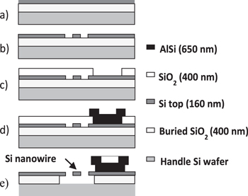
Figure 1. Flow chart of the nanowire devices fabrication process.
Download figure:
Standard image High-resolution imageIt is first uniformly doped by Boron implantation (NA = 1.5 × 1019 cm−3) and annealed at high temperature (figure 1(a)). Then it is patterned by a hybrid lithography followed by reactive ion etching (RIE): the anchor pads are patterned by deep ultraviolet (DUV) lithography while the nanowires are patterned by electron beam lithography (figure 1(b)). A SiO2 protective and insulating layer is subsequently deposited and patterned by UV lithography and RIE etching to open contact holes (figure 1(c)). A thick AlSi film is then deposited and patterned to form metallic electrodes on the anchor pads (figure 1(d)). Finally, the nanowires are released by vapor HF etching of the protective and buried SiO2 layers (figure 1(e)). This process was applied to the fabrication of devices with 160 nm thick nanowires having a length L in the 2.5–5.2 μm range, a width w in the 80–260 nm range, a L/w ratio in the 10–30 range and an orientation along the 〈110〉 crystallographic direction. An example of scanning electron microscopy (SEM) picture of a fabricated device is shown in figure 2 with a zoom in the nanowire area. Contrary to nanowires fabricated by the VLS method, these nanowires have a rectangular cross section. They likely exhibit greater sidewalls roughness resulting from the patterning techniques but their geometry is well mastered as well as their alignment and anchoring to contact pads. The experimental techniques that were developed for thermal and electromechanical characterizations of these nanowires are described in the next sections.

Figure 2. SEM picture of a 4 μm × 200 nm × 160 nm Si nanowire device.
Download figure:
Standard image High-resolution image2.2. Thermal conductivity measurements
The nanowires' thermal conductivity was measured by the 3 ω method [22]. In this method a sinusoidal current I(ω) with a radial frequency ω is injected in the nanowire under test. This induces a heating by joule effect at a radial frequency 2 ω and a partial modulation of the nanowire temperature at the same frequency. For small temperature changes ΔT = T − T0 where T0 is the ambient temperature, the nanowire resistance is a linear function of temperature at any position x along the nanowire so the resistance variation profile is also varying at twice the radial frequency ω. The resulting voltage drop V = RI has then 2 components: one large component V1ω related to ohm law with mean resistance variation, and a much smaller component at radial frequency 3 ω. At low modulation frequency, the thermal response is not limited by the thermal constant of the nanowire. It can be shown that for our nanowires, this condition is fulfilled if the current modulation frequency is much lower than a few MHz. Then the RMS value of the third harmonic of the voltage drop is given by [24]:

where IRMS is the RMS value of injected current, R0 the nanowire resistance at T0, α the linear temperature coefficient of resistance (TCR), κ the thermal conductivity at nanowire mean temperature, and S is the area of the nanowire cross section.
Equation (1) was established by assuming heat transport by Fourier's law. It shows that if thermal transport is diffusive, the thermal conductivity can be computed from measured values of V3ω, R0 and α. All our measurements were performed in the vacuum chamber (background pressure <10−5 mbar) of a cryogenic probe station Janis ST-500. A dc or ac current was injected in the nanowire device under test with a Keithley 6621 DC/AC l fA-100 mA current source. Static voltage measurements V(I) were performed with a Keithley 2182 nanovoltmeter while V3ω measurements were performed with a Signal Recovery 7280 lock-in amplifier. For the nanowires investigated here, the V1ω/V3ω ratio is in the 103–104 range and if a standard lock-in detection scheme is used, the input of the lock-in amplifier can be easily saturated by the 1 ω component of the signal. This can be avoided by using a very low injected current but a long integration time is then required to get measurable values of V3ω [21].
In order to use larger injected currents and thus get faster and lower noise measurements, the V1ω component of the signal must be reduced or removed before detection. This is often realized by a Wheatstone bridge configuration but this solution generates an unwanted parasitic 3 ω component in the injected current [25]. Instead we used a better performing cancellation circuit based on instrumentation amplifiers (figure 3). This circuit generates, from a shunt resistance in series with the nanowire, a voltage at radial frequency ω which is tuned and subtracted to the input signal of the lock-in amplifier. In addition the circuit was designed to allow a compensation of parasitic capacitances of the nanowire device which induces a phase lag in the 1 ω signal.
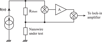
Figure 3. Simplified schematic drawing of the cancellation technique of the 1 ω signal.
Download figure:
Standard image High-resolution imageThe ac current injection also induces an increase of the mean temperature of the nanowire. This increase was estimated from an electrothermal modelling of the nanowire. If we assume that thermal transport is diffusive, the temperature profile can be calculated by solving the 1D heat diffusion equation with a Joule heating source and by considering nanowire ends at room temperature T0 as the boundary conditions. Because measurements are performed in vacuum, convection losses can be safely neglected. Radiative losses were also considered negligible because of the small nanowire area and the low temperature rises. The very good accuracy of this assumption and of a 1D model was checked by numerical solving the 1D heat equation including conduction and radiation losses and by comparison with 3D finite element simulations. We also checked that temperature variation of the resistance can be neglected for temperature profile calculations. With all these validated simplifying assumptions, it can be shown that the longitudinal temperature profile (along direction x) is simply given by the following simple expression [25]

where V = L × w × t is the volume of the nanowire. The maximum temperature at the midle of the nanowire (x = L/2) is then given by:

The temperature rise computed from equation (3) is plotted in figure 4 as a function of injected current for the highest and lowest resistivity nanowires investigated. To get low noise measurments while minimizing the temperature rise, all measurements were performed with an injection in the 10–60 μA range.
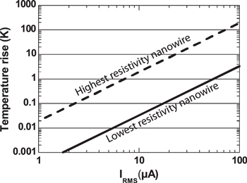
Figure 4. Computed temperature rise for the investigated Si nanowires as function of the RMS value of injected current.
Download figure:
Standard image High-resolution imageThe validity of the 3 ω method and the performances of our measurement set-up were checked from a measurement at room temperature on a 2.5 μm long, 260 nm wide and 160 nm thick boron doped Si nanowire (NA = 1.5 × 1019 cm−3). Measured values of the nanowire resistance R0 and α for this nanowire are 1.5 kΩ and 7 × 10⁻⁴ K−1, respectively. The variation of V3ω with the injected current for a modulation frequency equal to 1.007 kHz is displayed in figure 5. This frequency was chosen to be much lower than the cut-off frequency of the thermal response and not a multiple of power supply frequency (50 Hz). The inset in figure 5 shows that the variation V3ω with the cube power of injected current is highly linear in agreement with equation (1). The computed value of the thermal conductivity is 140 W m−1 K−1 which is close to the value for bulk silicon with the same doping level (130 W m−1 K−1).

Figure 5. Third harmonic of voltage drop versus injected current measured for a 160 nm thick, 250 nm and 2.5 μm long Si-p nanowire. R = 1.5 kΩ; α = 7 × 10⁻⁴ K−1. Inset: V3ω versus I03 and linear fit.
Download figure:
Standard image High-resolution image2.3. Piezoresistivity measurements
Bending of the substrate and measurement of the resulting device resistance variation is the most common technique for piezoresistance or piezoresistivity measurements of strain gauges made in nanomaterials. We considered that the following conditions should be fulfilled to get high quality and complete measurements by this technique:
- (i)A direct application of stress on the nanowire die. In most works, the method used to apply stress on the nanowire under test is bending of a plate on which the nanowires die is glued. Such indirect bending produces a stress field transmitted to the nanowire die which is largely dependent on the glue layer stiffness and which can be inhomogeneous. Consequently a reference strain gauge must be integrated in the nanowires die to get accurate, although relative, measurements,
- (ii)The ability to apply a static or a dynamic stress. Indeed, a dynamic stress loading was found necessary to avoid resistance variations due to charges exchanges between native oxide trap and bulk of Si nanowires which can lead to an apparent giant piezoresistance [4],
- (iii)An homogeneous stress field in a sufficiently large area to allow a comparison of a set of nanowires with various dimensions and fabricated in the same run,
- (iv)Measurements as function of temperature to get temperature coefficients of piezoresistivity,
- (v)Measurements in vacuum to avoid resistance variations due to humidity or other adsorbed species and to avoid thermal exchanges by convection.
In this work, the piezoresistance measurements were performed with the set-up depicted in figure 6 which follows these recommendations. It is based on in situ four point direct bending of the nanowire die in the vacuum chamber of the same cryogenic probe station as for thermal conductivity measurements described above. As expected, this system allows simultaneous application of a tensile stress on nanowires and measurements under probes of their resistance. The additional benefits of this system are its operation in vacuum (≤10−5 mbar) and its ability to allow dynamic stress loading, measurements below and above room temperature (from 200 K to 400 K), as well as a simultaneous optical visualization or measurement. More details on the set-up design and mechanical modelling can be found in [26] and its operation and characteristics will only be summarized here. The silicon die mechanical loading is obtained by an external large range (180 μm) and large maximum force (500 N) piezoelectric actuator with an embedded strain sensor for close loop control. This actuator pushes, with the help of two columns, an aperture rigid frame holding the fixed outer loading rods of the four point bending system. The inner bottom rollers of the four point bending system are supported by a tilting mechanical part which rests on button force sensor. The force sensor manufacturer electronics was replaced by a home-made low current electronics to avoid excessive sensor heating which prevented operation at low temperature. Tests with calibrated weights showed that the force sensor can then be operated at temperatures down to 200 K. Measurements at lower temperatures can be performed by replacing force measurement by an optical measurement of the die deformation [26]. The set-up was designed to minimize loading and supporting rods misalignments and asymmetries. For an ideal and symmetric four point bending system, the uniform surface stress generated in the area between inner supporting bars is given by:

where WD and tD are, respectively the width and thickness of the die, a is the distance between outer and inner bars (see figure 6), and F is the applied force. In the developed system a = 8.5 mm and a surface stress higher than 250 MPa can be applied on a 20 mm × 20 mm × 725 μm Si(100) die. This stress value is in the range of bending fracture strength values that we measured for such dies (217–540 MPa) in agreement with the ones reported for 525 μm thick polished Si wafers [27].
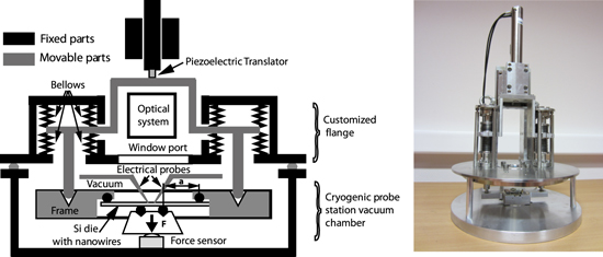
Figure 6. Schematic drawing and picture of the set-up allowing in situ four point bending of a Si die inside a cryogenic probe station.
Download figure:
Standard image High-resolution imageAn example of nanowire piezoresistance measurement at room temperature is shown in figure 7. It shows that the piezoresistance is highly linear in the investigated stress range (0–50 MPa) and that good quality measurements in terms of noise and stability can be achieved with the developed set-up.
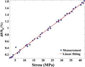
Figure 7. Piezoresistance of a Si-p nanowire versus applied surface stress. Nanowire dimensions L × w × t = 2.5 μm × 260 nm × 160 nm. R = 9650 Ω.
Download figure:
Standard image High-resolution image3. Results and discussion
3.1. Thermal conductivity of Si-p nanowires
Equation (1) above shows that thermal conductivity measurements by the 3 ω method require additional static measurements of the nanowire resistance and of the temperature coefficient of resistance (TCR) α. Despite some scattering of measured values, some general trends could be observed. When the nanowire size was reduced, its resistance was found to increase faster than the variation expected from a purely geometrical variation in agreement with a larger effect of depletion width due to positive surface charges. The temperature dependence of the resistance was found linear in the 200–380 K range although some departure from linearity could not be excluded for the narrowest (80 nm) nanowires. A trend towards an increase of the TCR when the nanowire width is decreased and possibly when the nanowire length is increased was observed (see table 1) but no well-defined dependence could be evidenced. Consequently, as a first approximation, the average value α = 7.6 × 10⁻⁶ K−1 was used for the evaluation of thermal conductivity from 2 ω measurements of nanowires with different dimensions.
Table 1. Temperature coefficient of resistance of Si-p nanowires with different lengths L and widths w. Average value: α = 6.7 × 10⁻⁴ K−1. Thickness: 160 nm. Doping NA = 1.5 × 1019 cm−3.
| w (nm) | 80 | 140 | 140 | 200 | 200 | 200 | 260 |
| L (μm) | 5.2 | 2.8 | 2.5 | 2.5 | 2.5 | 4 | 5.2 |
| α (×10−3 K−1) | 1.13 | 1.1 | 0.58 | 0.36 | 0.51 | 0.28 | 0.77 |
Our experimental results consistently showed that the behavior of the third harmonic of the voltage drop was well described by equation (1) for the investigated nanowires. This shows that heat conduction in the measured devices obeys Fourier's law of heat conduction as this is the basic assumption of the 3 ω method. In semiconductors, heat conduction can generally proceed through the motion of charge carriers and through the propagation of phonons related to lattice vibrations. In the case of silicon, heat conduction is generally dominated by phonon transport and is known to decrease with doping. So thermal transport by diffusion is not obvious because in nanowires the mean free path of phonons can be larger than nanowire dimensions, notably its cross section. In that case ballistic transport can occur and the 3 ω method becomes questionable. Our results show that inelastic phonon scattering at the walls of the nanowires is likely sufficiently high and the nanowires sufficiently long to get a heat transport limited by diffusion. This could be different for nanowires with smoother side walls, such as nanowires etched by silicon anisotropic chemical etching limited by crystal planes.
Our results of thermal conductivity measurements are shown in figure 8. As expected, they consistently show a large decrease of thermal conductivity compared to bulk silicon value when the nanowire width is reduced. Comparison with published work shows that values are lower than those of thin Si films [19] but larger those of VLS nanowires having a similar width but lower thickness [28].

Figure 8. Thermal conductivity of boron doped 〈110〉) Si nanowires with various dimensions (a) as a function of ambient temperature and (b) at 300 K as a function of nanowire width, and comparison with bulk silicon (dashed line). Nanowire thickness: 160 nm, boron doping: NA = 1.5 × 1019 cm−3.
Download figure:
Standard image High-resolution image3.2. Piezoresistivity of Si-p nanowires
The longitudinal piezoresistive coefficients πL of Si-p (100) nanowires aligned along 〈110〉 direction with different widths have been measured as a function of temperature. It was extracted from the measured relative variations of resistance ΔR/R and the longitudinal stress values σ computed from equation (4) by using the following equation:

If geometrical piezoresistance effect is neglected, for a p-type silicon nanowire oriented along 〈110〉 direction, πL is related to the coefficients πij of the piezoresistive tensor in the crystallographic coordinate system by:

where the second approximate equality comes from the much lower values of π11 and π12 with respect to π44 in p type doped silicon [29]. All measured nanowires had the same width (160 nm) and the same boron dopant concentration (1.5 × 1019 cm−3). The results of πL measurements are compared with values for bulk silicon and the same doping level in figure 9. These raw data show an increase of the piezoresistive coefficient of the nanowires when their width is reduced below about 260 nm. This would indicate that a slight giant piezoresistance effect is observed despite the high doping level and the relatively large sizes of the nanowire cross section. Let us emphasize that a dynamic stress loading at 0.02 Hz was applied for these measurements. According to [4], a giant piezoresistance effect should not be observable in this condition as it is mainly due to the variation of Si depletion width near the surfaces due to stress-induced charge exchanges between silicon and slow water traps in the native oxide. Our values are measured in vacuum, thus without humidity, but, like in all other published works, they are likely overestimated by a factor decreasing with nanowire width because of a variable stress concentration. This stress concentration is expected because of the width difference between the Si part released by lateral underetching near the anchors and the nanowire. For a width reduction by a factor 3.25 (from 260 nm to 80 nm) the ratio of piezoresistive coefficient is also close to 3. Finally, figure 9 also shows that the temperature coefficient of the longitudinal piezoresistive constant of Si nanowires is similar to the one of bulk silicon with the same doping level (−0.9 TPa K−1) [29] and only weakly variable with nanowire width.

Figure 9. Compilation of measured longitudinal piezoresistive coefficients versus temperature of Si-p 〈110〉 nanowires with different widths and comparison with bulk silicon. Nanowires thickness: 160 nm, Boron dopant concentration 1.5 × 1019 cm−3.
Download figure:
Standard image High-resolution image
4. Conclusion
In this work we measured the thermal conductivity and longitudinal piezoresistive coefficient of silicon nanowires fabricated by surface machining of an (100) SOI wafer and aligned along 〈110〉 direction. The thermal conductivity was measured in vacuum by the 3 ω method with relatively large driving currents owing to the implementation of a cancellation circuit of the 1 ω component of the signal. Measurements show that heat conduction in 80–260 nm wide, 160 nm thick and a few μm long nanowires follows Fourier's law likely because of the inelastic scattering on slightly rough sidewalls. Despite a scattering of the data due to variations of initial resistance and TCR values, a large decrease of the thermal conductivity was unambiguously observed when the nanowire size was reduced. Piezoresistance measurements were performed by a four point die bending system implemented in situ in a cryogenic probe station. The size effect on nanowire piezoresistance was found limited when a dynamic stress loading was applied. This supports the assumption that a large giant piezoresistance effect can only be observed in static mode.
Acknowledgments
This work was supported by the French ANR project 'ARIANE' (ANR-08-NANO-046) and is part of the PhD thesis of P E Allain supported by a grant of the French ministry of research. The authors wish to thank A C Rowe from Ecole Polytechnique (France) for fruitful discussions on the giant piezoresistance effect.
Footnotes
- *
Invited talk at the 7th International Workshop on Advanced Materials Science and Nanotechnology IWAMSN2014, 2–6 November, 2014, Ha Long, Vietnam