
Abstract
SnS in three nano forms possessing different morphologies such as particles, whiskers and ribbons were synthesised by chemical route. The morphology variation was brought about in the chemical route synthesis by varying a synthesis parameter such as temperature and influencing the synthesis by use of surfactant. The elemental composition determination by energy dispersive analysis of x-rays (EDAX) showed that all three synthesized SnS nanomaterials were tin deficient. The x-ray diffraction (XRD) study of the three SnS nanomaterials showed that all of them possess orthorhombic structure. The Raman spectra of the three SnS nanomaterials showed that all three samples possess three common distinguishable peaks. In them two peaks lying at 98 ± 1 cm−1 and 224 ± 4 cm−1 are the characteristic Ag mode of SnS. The third peak lying at 302 ± 1 cm−1 is associated with secondary Sn2S3 phase. The transmission electron microscopy (TEM) confirmed the respective morphologies. The optical analysis showed that they possess direct as well as indirect optical bandgap. The electrical transport properties study on the pellets prepared from the different nanomaterials of SnS showed them to be semiconducting and p-type in nature. The current–voltage (I–V) plots of the silver (Ag)/SnS nanomaterials pellets for dark and incandescent illumination showed that all configurations showed good ohmic behaviour except Ag/SnS nanoribbons pellet configuration under illumination. All the obtained results are discussed in detail.
Export citation and abstract BibTeX RIS

Original content from this work may be used under the terms of the Creative Commons Attribution 3.0 licence. Any further distribution of this work must maintain attribution to the author(s) and the title of the work, journal citation and DOI.
1. Introduction
Recently, research on the synthesis of compound semiconductor nanomaterials with specific morphologies has gained much attraction due to the dependence of optical and electrical properties on size and shape [1]. In the compound semiconductors, the IV–VI group binary compound SnS has received much attention as a potential candidate in photovoltaic devices, due to its remarkable stability, and interesting optical and structural characteristics [2, 3]. The other reason for SnS generating promising interest in optoelectronics is its nontoxic nature and that it possesses tuneable stoichiometry based bandgap lying within the visible range [4, 5]. It has room temperature optical band gap of 1.3 eV lying within visible range and also has a high-light absorption coefficient (>104 cm−1) [6]. According to the Shockley–Queisser criteria, a maximum efficiency up to 33% could be achieved for materials having Eg of 1.3 eV [7]. Intending to improve the light trapping ability and controlled electrical transport properties of SnS, researchers synthesised SnS in nano-scale with varying morphology. SnS in nano scale with different morphologies has been synthesized by diverse methods such as decomposition of a single source precursor [8], facile synthesis [9], solvothermal [10], hydrothermal [11] etc methods. Among these, simple chemical route is an effective method for SnS nano scale synthesis. By this method different morphologies and perfectly shaped nanostructures with high crystallinity can be synthesized. In this paper we report the synthesis of nano scale SnS possessing various morphologies by the simple chemical route. The morphology transformation was brought about in the chemical route synthesis by varying a synthesis parameter such as temperature and influencing the synthesis by use of surfactant. The SnS was synthesized in nanoparticles, nanowhiskers and nanoribbons forms by varying the synthesis parameters. The synthesized nano scale SnS were comprehensively characterized. The synthesis procedure and the obtained characterization results are deliberated in detail.
2. Experimental details
The SnS nano forms were synthesized by chemical route. All the chemicals used for the synthesis of SnS nanomaterials such as tin(II) chloride dihydrate (SnCl2 · 2H2O, Alfa Aesar, USA), triethanolamine (C6H15NO3, TEA, Loba Chemie, Mumbai, India), thioacetamide (CH3CSNH2, Loba Chemie, Mumbai, India), sodium sulfate (Na2S, qualigens fine chemicals, Mumbai, India), oxalic acid dihydrate (H2C2O4 · 2H2O, assay 98%, Chiti Chem Corporation, Vadodara, India), cetyltrimethyl ammonium bromide (CTAB, C19H42BrN, assay 98%, Chiti Chem Corporation, Vadodara, India) and aqueous ammonia (NH4OH, Merck, Mumbai, India) were of analytical reagent grade and used without further purification.
2.1. Synthesis of SnS nanoparticles
In the synthesis of SnS nanoparticles 1 g of SnCl2 · 2H2O was dissolved in 5 ml acetone by magnetic stirring. Then 5.5 ml of triethanolamine was added under constant stirring. Triethanolamine acts as a complexing agent and extracts Sn+2 ions from the solution. Under constant magnetic stirring, 0.3 g of thioacetamide as a source of sulfur is added. The pH of the final solution was made more than 7 by adding 5 ml of aqueous ammonia. It was felt that by keeping pH above 7 enhances the reaction speed between Sn+2 and S−2. The final solution of the bath was made 100 ml by adding distilled water. The final solution was kept at ambient temperature for 4 h. The solution gradually turned brown-black in color. The particles from the beaker were filtered out and given a multiple wash with double-distilled water and absolute methanol to remove impurity. After that they were dried in an oven at 45 °C for 2 h to get nanoparticles yield.
2.2. Synthesis of SnS nanowhiskers
In the typical synthesis of SnS nanowhiskers the same solution prepared for SnS nanoparticles synthesis was used. The only difference was that the final solution was held at 80 °C for 2 h instead of ambient temperature. The beaker containing the final solution was held at 80 °C employing a temperature controlled hot water bath. The solution immediately turned brown-black in color indicating the fast growth of SnS. The temperature led to fast growth and that might be responsible for the formation of whiskers rather than spherical particles. The precipitates from the beaker were filtered and given a multiple wash with double-distilled water and absolute methanol to remove the impurity. Later they were dried in an oven at 45 °C for 2 h to get nanowhiskers yield.
2.3. Synthesis of SnS nanoribbons
In the typical synthesis of SnS nanoribbons, firstly a clear solution of 350 ml of 4.4 mM CTAB was prepared in distilled water by magnetic stirring that worked as a surfactant. Subsequently, 0.02 M H2C2O4 · 2H2O and 0.01 mM SnCl2 · 2H2O was added to the solution of CTAB under constant magnetic stirring. Oxalic acid dihydrate was used as a reducing agent that forms the stannous oxalate (SnC2O4) after reacting with the stannous chloride. Then 0.01 mM Na2S · 9H2O aqueous solution is added drop by drop into the solution to get black suspension. This final solution is magnetically stirred for half an hour at ambient temperature. Finally, the black suspension is filtered and given a multiple wash with double-distilled water and methanol to remove impurities. After the multiple wash, they are dried in an oven at 45 °C for 2 h to obtain SnS nanoribbons yield.
2.4. Reaction mechanism
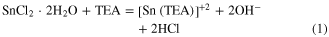
The chemical reactions occurring in the chemical route synthesis of SnS nanoparticles and nanowhiskers are as below:

The chemical reaction occurring in the chemical route synthesis of SnS nanoribbons is as below:

2.5. Characterizations
The elemental stoichiometric analysis of all the as-synthesized SnS nanomaterials samples was done by energy dispersive analysis of x-rays (EDAX) attached to JEOL JSM 5600 scanning electron microscope. The x-ray diffraction (XRD) patterns for all the as-synthesized nanomaterials samples were recorded using Bruker D8 advance x-ray diffractometer employing graphite monochromatized CuKα radiation (λ = 1.5405 Å). The scanning rate of 1.5 °C min−1 was applied to record the pattern in the 2θ range of 10–80 °. The room temperature Raman spectra were recorded using Jobin Yvon Horiba LABRAM-HR visible (He-Ne laser, 632.8 nm) spectrometer. The transmission electron microscopy (TEM) images and selected area electron diffraction (SAED) patterns were recorded using Philips, Tecnai 20 microscope by operating at an acceleration voltage of 200 kV. The samples for TEM analysis were prepared by mono dispersing respective samples in methanol by sonication. A drop was allowed to fall on carbon coated copper grids and the solvent was allowed to evaporate under ambient conditions. The excess solvent was removed by vacuum drying. The optical absorption response of all the as-synthesized SnS nanomaterials samples were studied using a UV–Vis–NIR spectrophotometer, Varian Cary 500, Shimadzu UV 3600, in the wavelength range of 300–1400 nm at room temperature. The electrical transport properties of the SnS nanomaterials were studied by preparing pellets under high pressure using respective nano samples. The current-voltage (I–V) plots in dark and incandescent illumination of Ag/nano SnS pellets configurations were measured using Agilent (U2777A) meter unit. The four probe dc electrical resistivity of the nanomaterials pellets in the temperature range of ambient to 393 K was carried out employing four probe setup Model-DFP02 developed by Scientific Equipment Services (SES), Roorkee, India. The Hall effect measurements at room temperature employing van der Pauw configuration were carried out on pellets prepared by nanomaterials using the Hall effect set-up model-DHE22 together with constant current source Model-DPS175 developed by SES, Roorkee, India.
3. Results and discussion
The EDAX analysis of the as-synthesized SnS nanomaterials shows the presence of Sn and S elements only. The atomic percentages of the elements obtained from the EDAX analysis are tabulated in table 1. The Sn-to-S atomic percentages ratio observed are 0.85 for SnS nanoparticles, 0.83 for SnS nanowhiskers and 0.97 for SnS nanoribbons. The ratio states that all three synthesized SnS nanomaterials are tin deficient.
Table 1. EDAX data of as-synthesised SnS nanomaterials.
| Atomic percentages (at.%) of elements | ||||
| Standard | Experimental | |||
| Compound SnS | Sn | S | Sn | S |
| Nanoparticles | 50 | 50 | 46.36 | 53.64 |
| Nanowhiskers | 50 | 50 | 45.44 | 54.56 |
| Nanoribbons | 50 | 50 | 49.30 | 50.70 |
The x-ray diffraction patterns of as-synthesized SnS nanomaterials, figure 1, show that all the diffraction peaks are at nearly the same 2θ values for nanoparticles, nanowhiskers and nanoribbons. All the diffraction peaks could be indexed as those of orthorhombic SnS. The lattice parameters, table 1, were in good agreement with the reported data [JCPDS: 39-0354]. The morphology variations do not affect the XRD, except for a minor variation of ±1° shift in the 2θ positions in the case of nanowhiskers. This may be due to high temperature synthesis of nanowhiskers, which caused higher strain leading to minor 2θ variations.

Figure 1. X-ray diffraction patterns of the as-synthesized SnS nanomaterials.
Download figure:
Standard image High-resolution imageThe crystallite size (L) was calculated using Debye–Scherrer's formula for different x-ray reflections [12]

where K is the shape factor (taken as 0.9), λ is the wavelength of x-ray (1.5405 Å), β is the angular line width at half maxima intensity of XRD peaks and θ is the Bragg angle in degree. The average crystallite sizes estimated from the XRD analysis using Scherrer's formula are tabulated in table 2.
Table 2. XRD parameters of as-synthesized SnS nanomaterials.
| Parameters | Nanoparticles | Nanowhiskers | Nanoribbons |
|---|---|---|---|
| Lattice parameters/Å | a = 4.329, b = 11.190, c = 3.983 [JCPDS: 39-0354] | ||
| Crystal structure | Orthorhombic | ||
| L nm, (Scherrer's formula) | 10.01 | 12.41 | 13.75 |
| L nm, (HW plot) | 9.29 | 11.16 | 13.33 |
Strain  (×10−3) (×10−3) |
−1.58 | −4.37 | −0.38 |
| Dislocation density δ × 10−3 (Lin·nm−2) | 11.6 | 9.69 | 5.63 |
The average crystallite size (L) and the micro strain () in the as-synthesized SnS nanomaterials were estimated by Hall–Williamson [13] relation

The Hall–Williamson (HW) equation incorporates the Scherrer's formula of crystallite size and the micro strain terms. Here β is full width at half maxima (FWHMs) of the diffraction peaks.
The plots of  versus
  for the as-synthesized SnS nanomaterials are shown in figure 2. In contour to equation (5), the plots are a straight line in which the reciprocal of an intercept on
  axis gives the average crystallite size and the slope gives the residual strain. The crystallite sizes obtained from the Scherrer's relation and HW plots were in good agreement with each other. The crystallite size of the nanoparticles was found to be smaller than nanoribbons and nanowhiskers. The residual strain values obtained from the slope of the HW plots are tabulated in table 2. All the values are negative stating it to be compressive strains. The highest value of compressive strain is in the case of nanowhiskers and lowest in the case of nanoribbons. This clearly indicates that high temperature induces strains which lead to nanowhiskers formation [14, 15], while surfactant leads to formation of nanoribbons with least strains.

Figure 2. Hall–Williamson plots of as-synthesized SnS nanomaterials.
Download figure:
Standard image High-resolution imageUsing crystallite size values, the dislocation density (δ), defined as the length of dislocation lines per unit volume in the nanomaterials was calculated using Williamson and Smallman's formula [16]

The obtained values of the dislocation density (δ) are tabulated in table 2. The values show that it is lowest in the case of the nanoribbons followed by nanowhiskers and nanoparticles. That means the use of surfactant and high temperature of 80 °C in the synthesis of nanoribbons and nanowhiskers respectively, reduces the dislocation density (δ). This clearly indicates that surfactant and temperature enhance crystallization in SnS nanomaterials, thus increasing the crystallite size and reducing the dislocation density, making it a potential candidate for optoelectronic devices [17].
The Raman spectra of as-synthesized SnS nanomaterials are shown in figure 3. The spectra shows that there are three distinguishable peaks lying at 98 ± 1, 224 ± 4 and 302 ± 1 cm−1. The 98 ± 1 cm−1 and 224 ± 4 cm−1 peaks are the characteristic Ag mode of SnS [18, 19]. These peaks arise due to inter atomic vibration between metal (Sn) and chalcogen (S). The 302 ± 1 cm−1 peak is associated with secondary tin sulphide phase, Sn2S3 [20]. This Raman peak ascertains that the as-synthesised SnS possesses secondary tin sulphide phase Sn2S3 as impurity. This may be arising from the intra-layer vibration of chalcogen–chalcogen [20].

Figure 3. Raman spectra of as-synthesized SnS nanomaterials.
Download figure:
Standard image High-resolution imageThe transmission electron microscopy (TEM) images of the as-synthesized SnS nanomaterials are shown in figure 4. The images clearly show variation in the morphology. The TEM image of figure 4(a) clearly shows that SnS particles are spherical in shape with average diameter of 12 nm. The TEM image in figure 4(b) clearly states that the synthesized SnS consists of whiskers having average length below 100 nm and width 14.71 ± 1 nm. According to the basic phenomenon, the presence of compressive residual strain is the main driving force of the whisker formation [14, 15]. Table 2 shows that SnS nanowhisker has highest compressive strain value, thus indicating that strain leads to whisker formation. Figure 4(c) shows the TEM image of synthesized SnS nanoribbons in which the nanoribbons have average length above 100 nm and width of 11 ± 1 nm. Thus, the TEM images of the nanomaterials confirmed different morphologies of the as-synthesized SnS.

Figure 4. TEM images of as-synthesized SnS (a) nanoparticles, (b) nanowhiskers and (c) nanoribbons.
Download figure:
Standard image High-resolution imageThe selected area electron diffraction (SAED) patterns of the as-synthesized SnS nanomaterials are shown in figure 5. The SAED pattern of nanoparticles is shown in figure 5(a) which shows rings clearly stating polycrystalline nature. The SAED patterns of nanowhiskers and nanoribbons are shown in figures 5(b) and (c), respectively. They have bright spots lying on the rings indicating improvement in crystallinity. Thus, crystallinity increases in the case of nanowhiskers and nanoribbons compared to nanoparticles. This confirms that high temperature and use of surfactant in the synthesis process leads to high crystallinity of the nanomaterials. All the SAED rings of the as-synthesized nanomaterials could be indexed as those of orthorhombic SnS structure. The indexed SAED planes are in good agreement with the respective x-ray diffraction planes.

Figure 5. The SAED patterns of as-synthesized SnS (a) nanoparticles, (b) nanowhiskers and (c) nanoribbons.
Download figure:
Standard image High-resolution imageThe optical absorbance spectra of SnS nanomaterials were recorded by taking mono dispersed respective nanomaterials in methanol as samples and plain methanol as reference. The obtained spectra are shown in figure 6(a). All the nanomaterials show broad optical absorbance in the optical range of 300–1100 nm. Figure 6(b) shows the optical absorption coefficient spectra. It clearly states that all the as-synthesised SnS nanomaterials had high optical absorption coefficient lying in the range of 106 cm−1 [6]. The broad optical absorbance and high optical absorption coefficient are observed throughout the visible range making the synthesised SnS nanomaterials with different morphology to be potential candidates as absorber material in solar cell.

Figure 6. As-synthesized SnS nanomaterials (a) absorbance spectra, (b) absorption coefficient spectra, (c) (αhν)2 versus hν plots and (d) (αhν)1/2 versus hν plots.
Download figure:
Standard image High-resolution imageThe energy bandgap Eg was determined from the optical absorption data using the near-band edge absorption relation [21]

where n characterizes the transition. For direct allowed and forbidden transitions, n = 2 and 2/3 respectively, and n = 1/2 and 1/3 for indirect allowed and forbidden transitions, respectively. The absorption coefficient α was calculated employing the below relation [21]

where A is the absorbance of the light through sample, ρ is the density of SnS taken here as that of solid SnS (5.1 g cm−3) [22], c is the sample concentration dispersed in acetone, M is the molecular weight of SnS and l is the path length of light.
The analysis of equation (7) showed that, n = 2 and 1/2 fitted for the as-synthesized SnS nanomaterials confirming the presence of direct and indirect allowed transitions in the SnS nanomaterials. The values of direct and indirect optical bandgap of synthesized SnS nanomaterials were determine from the plots of (αhν)2 versus hν, figure 6(c), and (αhν)1/2 versus hν, figure 6(d), respectively. The obtained values are tabulated in table 3. The direct bandgap values of nanoparticles came out to be 1.42 eV and that of nanoribbons to be 1.31 eV. These values of direct optical bandgap were found to be higher than the bulk SnS bandgap of 1.3 eV [23]. This clearly indicates blue shift arising due to size effect. The direct optical bandgap of nanowhiskers came out to be 1.15 eV, which was less than the bulk SnS bandgap value, stating red shift. This may be arising due to changes in the electronic structure of SnS due to the presence of large deformation strain [4].
Table 3. Optical and electrical transport properties parameters.
| Parameters | Nanoparticles | Nanowhiskers | Nanoribbons | |
|---|---|---|---|---|
| 314–364 K | 0.18 | 0.22 | 0.21 | |
| Ea (eV) | 365–393 K | 0.15 | 0.19 | 0.29 |
| ρ × 105 (Ω cm) at 309 K | 6.59 | 4.06 | 0.69 | |
| RH (cm3 C−1) (×106) | 12.02 | 7.42 | 1.25 | |
| Type of conduction | p | p | p | |
| μH (cm2 V−1 sec−1) | 18.74 | 115.09 | 40.28 | |
| p (cm−3) | 5.20 × 10¹¹ | 8.43 × 10¹¹ | 4.99 × 10¹² | |
| Eg (eV) | Direct | 1.42 | 1.15 | 1.31 |
| Indirect | 0.68 | 0.63 | 0.64 | |
The values of the indirect optical bandgap varied from 0.63 eV for nanowhiskers, 0.64 eV for nanoribbons to 0.68 eV for nanoparticles. These values are lower than the reported indirect bandgap value of 1.0 eV [24, 25]. This deviation from the reported value may be due to different methods of synthesis and varied morphology.
The electrical transport properties, such as dc electrical resistivity variation with temperature, I–V characteristics for different illuminations and ambient condition Hall effect studies were carried out on pellets prepared by hydraulic pressing of SnS nanomaterials. For pellets preparation, 3 g of as-synthesized SnS nanomaterials each were uniformly loaded in die and pressed in a hydraulic press to 0.5 GPa for 30 min. The obtained pellets were of 1.4 cm diameters and nearly 800 μm thicknesses.
Figure 7(a) shows the dc electrical resistivity variation with temperature of the as-synthesized SnS nanomaterials pellets. The measurements were done in the temperature range from ambient to 393 K. It is seen that in each nanomaterials pellets the dc resistivity value decreases with increase in temperature stating the nanomaterials to be semiconducting in nature.

Figure 7. Plots of (a) electrical resistivity versus temperature and (b) Ln(σ) versus 1000 T−1.
Download figure:
Standard image High-resolution imageThe plots of conductivity ln(σ) versus 1000 T−1 are shown in figure 7(b). All the plots show that there exist two slopes acknowledging two values of the activation energy. The activation energy values were determined from the relation of electrical conductivity (σ) and temperature given by the Arrhenius equation

where Ea is the activation energy, σ0 is the conductivity pre-exponential factor. The values of Ea obtained by the least square fit of the experimental data, figure 7(b), are tabulated in table 3. The activation energy values vary from 0.15 eV to 0.29 eV for different SnS nanomaterials.
The current-voltage (I–V) characteristic study was undertaken on the pellets prepared from the three SnS nanomaterials by taking contact using silver (Ag). The I–V characteristic measurements of the Ag/SnS nanomaterials pellets configurations were done in the voltage range of ±20 V (figure 8). The I–V characteristics were measured for dark as well as for incandescent illumination intensity of 100 W cm−2 on the surface of Ag/SnS nanomaterials pellets. The I–V measurements were recorded using Agilent (U2777A) source meter unit. The measurements showed that the current linearly increases with voltage for Ag/SnS nanoparticles and nanowhiskers pellets configuration in the voltage range of ±20 V having r2 > 0.99 indicating the silver contacts on the films were ohmic. The Ag/SnS nanoribbons pellet configuration showed the I–V curve linearity of ohmic behavior for dark having r2 > 0.99. But Ag/SnS nanoribbons pellet configuration under incandescent illumination showed diode like behavior. The I–V characteristics were recorded for three samples (pellets) each. All the characteristics had minor deviations but their nature remained same. The Ilight/Idark ratio of the Ag/SnS nanoparticles, nanowhiskers and nanoribbons pellets at ±15 V is about 2.18, 2.18 and 5.03, respectively, which is much higher than the reported values for chemically deposited SnS thin films [26, 27]. The obtained large value of Ilight/Idark ratio of the Ag/SnS nanomaterials pellets configuration arises due to morphological variation contending that the as-synthesized SnS nanomaterials can have varied potential application in photovoltaic devices.

Figure 8. The I–V characteristics of Ag/SnS nanomaterials pellets.
Download figure:
Standard image High-resolution image
The ambient temperature Hall effect measurements were performed on the pellets of the as-synthesized SnS nanomaterials by taking ohmic contacts using silver paste in van der Pauw geometry. The Hall coefficient, mobility and charge carrier concentration of the samples were evaluated using the relations


The values of the carrier concentration obtained for the three SnS nanomaterials pellets, table 3, are near to the semiconductor carrier concentration. The magnitude of the carrier concentration values in the case of nanomaterials pellets is slightly less than the ideal semiconductor carrier concentration. This may be due to non firing of the pellets. In pellets without heat treatment there will be a lack of coalescence between the nano scales SnS hindering free movement of charge carriers within the pellet, thus showing lesser carrier concentration values. The comparative values of the carrier concentration show that it is large in the case of pellets prepared by SnS nanowhiskers and nanoribbons than nanoparticles. The ambient temperature (309 K) dc electrical resistivity values were also less in the case of pellets prepared by nanowhiskers and nanoribbons compared to pellets prepared from nanoparticles. These results might be due to high crystallinity observed in SnS nanowhiskers and nanoribbons observed from SAED patterns. Also, larger length of whiskers and ribbons than particles gives larger carrier mobility in whiskers and ribbons compared to particles. The positive value of the Hall coefficient confirms the p-type nature of the as-synthesized SnS nanomaterials. The p-type nature of the pellets prepared using as-synthesized SnS nanomaterials is due to the acceptor levels created by the tin vacancies in the lattice owing to tin deficiency [28]. The tin deficiency in the as-synthesized SnS nanomaterials was confirmed by the respective EDAX analysis data. From the Hall effect measurements data, table 3, one can state that the high synthesis temperature enhances the mobility of the SnS nanowhiskers compared to nanoparticles and nanoribbons.
4. Conclusions
Nano size SnS having different morphologies viz nanoparticles, nanowhiskers and nanoribbons has been synthesized by simple chemical route. The chemical solution used for the synthesis of nanoparticles and nanowhiskers was the same. The difference was in the synthesis temperature employed. The nanoparticles were synthesised at ambient condition and nanowhiskers were synthesised at 80 °C, while in the synthesis of SnS nanoribbons, surfactant CTAB was used. The high temperature of 80 °C and use of surfactant CTAB in the synthesis led to the formation of nanowhiskers and nanoribbons, respectively. The EDAX analysis of all three as-synthesized SnS nanomaterials indicates that they are tin deficient. The XRD analysis showed that the three as-synthesised SnS nanomaterials possess orthorhombic structure. The lattice parameters were in good agreement with the reported data. The crystallite size determined from the XRD data using Scherrer's formula and Hall–Williamson relation states that the nanowhiskers and nanoribbons have slightly larger crystallite sizes than nanoparticles. The slight increase in the crystallite size of the nanowhiskers and nanoribbons is due to high temperature and use of surfactant in the synthesis processes, respectively. The Raman spectra of the three as-synthesised SnS nanomaterials showed that all the samples exhibit three common distinguishable peaks. Of these, the two peaks lying at 98 ± 1 cm−1 and 224 ± 4 cm−1 are the characteristic Ag mode of SnS, whereas the third peak of 302 ± 1 cm−1 is associated with secondary tin sulphide phase Sn2S3. The TEM images of the three as-synthesized SnS nanomaterials showed that they possess respective morphologies of nanoparticles, nanowhiskers and nanoribbons. The SAED pattern of the three SnS nanomaterials indicates that nanowhiskers and nanoribbons possess greater crystallinity than nanoparticles. The increase in crystallinity in nanowhiskers and nanoribbons is attributed to high temperature synthesis at 80 °C and use of CTAB surfactant, respectively. The as-synthesized SnS nanomaterials showed broad optical absorbance and high optical absorption coefficient of 106 cm−1 in the analyzed wavelength range of 300 to 1100 nm. The evaluated direct optical energy bandgap values showed that nanoparticles (1.42 eV) and nanoribbons (1.31 eV) have higher direct optical bandgap values than reported bulk SnS direct optical bandgap (1.3 eV). This means that nanoparticles and nanoribbons show blue shift due to size effect. However, nanowhiskers direct optical bandgap value (1.15 eV) is less than reported bulk SnS value (1.3 eV), indicating red shift arising due to large value of deformation strain arising owing to high synthesis temperature. All three SnS nanomaterials also possess indirect optical bandgap values, 0.63 eV by nanowhiskers, 0.64 eV by nanoribbons and 0.68 eV by nanoparticles The electrical transport properties studies such as dc electrical resistivity variation with increase in temperature, I–V plots under dark and incandescent illumination along with ambient condition Hall effect studies were carried out on pellets prepared from the respective three SnS nanomaterials under high pressure. The dc resistivity variation with temperature study showed that the dc resistivity value decreases with increase in temperature indicating that all three nano samples are semiconductors. The I–V plots in dark and under incandescent illumination (100 W cm−2) of silver (Ag)/SnS nanomaterials pellets configurations, except for Ag/SnS nanoribbons pellet under illumination, showed linear ohmic behaviour in dark as well as under incandescent illumination. The Ag/SnS nanoribbons pellet showed diode like behaviour. The Ilight/Idark ratio of the Ag/SnS nanoparticles, nanowhiskers and nanoribbons pellets at ±15 V is about 2.18, 2.18 and 5.03, respectively, which is much higher than the reported values for chemically deposited SnS thin films. The large value of Ilight/Idark ratio of the Ag/SnS nanomaterials pellets configuration shows its potential application in photovoltaic devices. The ambient condition Hall effect measurements on three SnS nanomaterials pellets corroborated the semiconducting nature. It also showed that the nanomaterials are of p-type nature.
Acknowledgement
All the authors are grateful to the Department of Atomic Energy (DAE)-BRNS, Mumbai, India for providing financial assistance through DAE-BRNS Major Research Project Sanction No. 2010/34/34/BRNS/2060 dated 13 December 2010 for carrying out this research. The authors are grateful to the UGC-DAE CSR, Indore for EDAX, XRD and Raman analysis. The authors are also grateful to the Sophisticated Instrumentation Centre for Applied Research and Testing (SICART) Vallabh Vidyanagar, Gujarat for TEM, SAED analysis and Central Salt and Marine Chemicals Research Institute (CSMCRI), Bhavnagar for UV–vis-NIR analysis of our samples.