
Abstract
Compared to the conventional silicon-based technology, the solution process appears to be a revolution in the field of micro/nanofabrication due to its advantages of high efficiency in material and energy consumption and the use of low cost material. In this paper, we introduce a new approach to fabricate BioMEMS devices using this novel technology to make microcavity. Zirconium oxide patterns were formed on the silicon substrate simply by spin coating its precursor and thermal imprinting technique. We used poly-propylene carbonate (PPC) for the sacrificial material due to its unique pyrolysis property. The PPC was coated on the ZrO patterns and excess film was etched by oxygen plasma but retaining PPC structure between the lines of ZrO pattern. Then another ZrO layer was coated to encapsulate the PPC. The final microcavity structures were obtained by just baking the substrate by pyrolyzing the PPC. The obtained results show the approach's prospect of becoming an ideal alternative for the current BioMEMS micro/nanofabrication technologies
Export citation and abstract BibTeX RIS

Original content from this work may be used under the terms of the Creative Commons Attribution 3.0 licence. Any further distribution of this work must maintain attribution to the author(s) and the title of the work, journal citation and DOI.
1. Introduction
BioMEMS, which is a particular type of microelectronmechanical system (MEMS), has been proven to have great potential in improving human quality of life. Since the first BioMEMS study was published in 1967, it has gone through developing periods to bring out commercialized products that indeed serve human life.
In a world where human demands in health and quality of life are increasing rapidly while resources are limited, the fact that BioMEMS has been developed based on silicon technology may constrain its future development and applications due to four main reasons. First, the efficiency of material usage is very low. BioMEMS devices are fabricated mainly by lithography-based process, which is composed of many cycles of deposition layers of materials then removing the unnecessary part to form patterns. The wasting portion of the deposited material can be up to 95%. Secondly, BioMEMS devices usually consume large amount of materials. While we can reduce the consumption of electronic materials for producing MEMS by reducing its size, in the case of BioMEMS devices we cannot. This is their unique disadvantage, since most of the BioMEMS devices have to be reasonably large enough to handle the sample and (sometimes) the reagent. Along with the high consumption of materials, the use of expensive materials such as silicon will also limit their application. Although, current mainstream materials of BioMEMS researches are plastics and polymers, which have low cost and can be easily fabricated, the stability in dimensions and chemicals are not sufficient for some important applications. Another important aspect which need considering is the use of energy, since the conventional process consumes a lot of energy for facilities and working medium (e.g. maintenance of vacuum equipment, clean room etc). As a result of those limitations, the imperative task is to find out an alternative technology for the future.
In order to overcome these problems, one prospective approach is the solution process [1–3]. In this novel technology, all materials are prepared in the solution then patterned using printing techniques such as imprinting, inkjet printing [4] and so on. The SHIMODA Nano-Liquid Process Project group has established this solution technique and has been obtaining many promising results. Compared with the conventional methods, the solution process appears to be an ideal replacement for the future. Combining with the use of low cost materials, it can maximize the efficiency of the usage of materials since all the deposited layers can be part of a fully worked-out device. Moreover, the consumption of energy can be reduced significantly because it is possible to perform the whole process under atmospheric pressure [3, 5].
While semiconductor devices simply consist of multilayers of deposited materials, conductive, insulator, and semiconductors, BioMEMS devices require mechanically active architectures such as cantilevers, pillars, diaphragms, and channels for flow. In this paper we show the attempt to enhance the applicability of the solution process to be compatible with manufacturing the above-mentioned structure.
Figure 1 illustrates the principle of our approach to fabricate the microcavities. In this paper, our idea is to use the solution process to fabricate one of the most basic structures in BioMEMS devices, the microcavity. Furthermore, our originality is the choices of the metal oxide (ZrO) to form the cavity structure which has lower cost (compared to Si) and is more stable in dimension (compared to plastics, polymers), and poly propylene carbonate (PPC), a new material which can be not only imprinted, but is also a perfect sacrificial material due to its clean pyrolysis property.
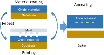
Figure 1. Schematic diagram of solution processing of microcavities.
Download figure:
Standard image High-resolution image2. Experimental
2.1. Materials
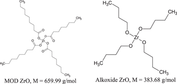
For the structure of cavities, we prepared two different types of ZrO solution. The first is the metal oxide decomposition (MOD) solution: zirconium 2-ethylhexanoate 90% (M = 659.99 g mol−1), and the other is alkoxide solution: zirconium tetra-n-butoxide (M = 383.68 g mol−1). Both of them were dissolved in propionic acid at ZrO concentrations of 0.3 mol kg−1. In these solutions, the MOD contains more organic component than the alkoxide solution, its Zr atom is surrounded by long carbon chains, which help to ease the imprinting step. In this process, we used the mixture of these two solutions at the ratio of 1:1 (in volume).
For the sacrificial layer, the PPC was prepared by dissolving in diethylene glycol monomethyl ether acetate (DGMEA) at a concentration of 6.25%.
2.2. Process
Figure 2 illustrates our process step-by-step to fabricate the microcavity. Our process comprises three main stages:
- Stage 1: the first ZrO layer is deposited on the substrate using spin coating then patterned by the nano-rheology printing process (n-RP)
- Stage 2: spaces between ZrO patterns are filled with PPC by coating a layer of PPC. Then excess PPC has been removed using O2 plasma etching.
- Stage 3: coating the 2nd ZrO layer and baking to form ZrO cavities.

Figure 2. Diagram of the fabrications of ZrO cavity based on n-RP process of ZrO gel.
Download figure:
Standard image High-resolution image2.3. Characterization
Atom force microscopy (AFM) was used to assess the morphology of the sample while scanning electron microscopy (SEM) helps to evaluate the shape of patterns. From these results, the parameters of the process were optimized.
3. Results and discussion
3.1. Stage 1: ZrO patterning by the n-RP process
These images show the obtained ZrO structure using the n-RP process (figure 3). Compared to the mold, having patterns' height of 350 nm, the ZrO patterns have the height of approximately 340 nm. This fact obtained from AFM implies that during imprinting, the ZrO gel almost fulfills the mould and the structure shape is maintained even after removal of the mould.
3.2. Stage 2: patterning the sacrificial layer
By comparing the AFM results of the samples before coating with PPC and those that were etched for various times, we can figure out the most appropriate etching time for our process.
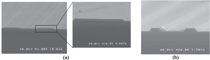
Figure 3. SEM images of obtained ZrO gel patterns; (a): 10 μm patterns; (b) 1 μm patterns.
Download figure:
Standard image High-resolution imageFigure 4 shows the shapes of patterns before coating with PPC and after etching at various times with oxygen plasma. Looking at the results after etching for 120 s and 150 s, the patterns are wavy, and the height of patterns is smaller than the height of those before coating, proving that PPC still remained on the patterns and the etching time had to be increased.
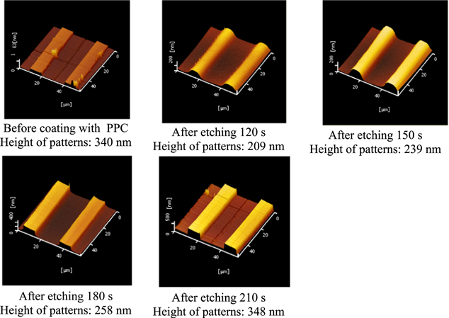
Figure 4. AFM results of patterns before and after various O2 plasma etching times.
Download figure:
Standard image High-resolution imageOn raising the etching time to 180 s, the ZrO patterns were exposed, demonstrated by the fact that the shape of patterns became rectangular just like those after imprinting. However, PPC still remained in the groove between patterns (the height of patterns is smaller than that of the before-coating-PPC sample). This is necessary because if there is any PPC left on the ZrO patterns, the first and second ZrO layers cannot form a bond between them. Hence, the removal of PPC in the next stage will also peel off the second ZrO layer. After etching for 210 s, we can conclude that the PPC was totally removed since now the height of patterns is similar to that of the before-coating-PPC sample. Therefore, we chose 180 s as the most suitable etching time for this stage.
3.3. Stage 3: coating the 2nd ZrO layer and baking to form ZrO cavities
Figure 5 shows the ZrO cavity after annealing to remove PPC. The result reveals some promising advantages of our process. First, apparently, the PPC was totally removed leaving a cavity without making any defect on the ZrO patterns, proving its ability to be a perfect sacrificial layer. Moreover, the second ZrO appears to be well bonded to the first layer. Conventional BioMEMS fabrication processes require complicated techniques to form the cavities such as fusion bonding, anodic bonding and so on. In this case, as the first ZrO was still in the gel form, the second ZrO easily formed the bonding just by coating by spin coating then drying. Although we have not performed any measurement to evaluate the bonding strength, it seemed to be acceptable enough since we had to cut the sample for SEM observation and the second layer was not peeled off. This is another strong point of the solution process in general and our process in particular.
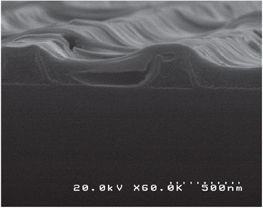
Figure 5. ZrO cavity in gel form.
Download figure:
Standard image High-resolution imageHowever, we could not perform the last step of the process, annealing the sample to crystallize the ZrO structure due to the shrinking of these structure after pre-annealing step to remove the PPC. This phenomenon happened because the organic component in these layers pylorized during annealing. Apparently, this issue can be overcome by reducing the portion of MOD solution which contributes much more organic component than the alkoxide solution (figure 6). Nevertheless, our experiments show that this reduction decreases the ZrO solution's ability to be imprinted and may affect the quality of the ZrO patterns.
Figure 6. Structures of two types of ZrO solution.
Download figure:
Standard image High-resolution image
4. Conclusion
In conclusion, we have obtained the microcavities using a completely new approach. Although we have an issue in the last step, which is for the crystallization of ZrO structures, its potential is undeniable. The materials for the process are metal oxide (ZrO) in solution, whose cost is much lower than some conventional materials such as silicon, and PPC, which is an ideal sacrificial material since the removal to form cavity structure is simple and clean without causing defects in the second ZrO layer. ZrO layers were coated, and patterned without using any vacuum equipment; even the plasma-etching step can be performed at atmospheric pressure. Moreover, the bonding between the first and the second ZrO layer can also be simply formed just by coating and drying. These advantages make this process highly promising for compatibility with the future in which lack of resources is a serious issue for our planet.
Acknowledgments
This work is the result of the cooperation between Vietnam National University (VNU) and Japan Advanced Institute of Science and Technology (JAIST) in general, between the Laboratory for Nanotechnology (LNT) and Green Devices Research Center (GDRC) in particular. The authors are grateful to Sumitomo Seika Chemicals CO., LTD (Japan) for providing the PPC.