
Abstract
In this paper, we report on the fabrication of blue GaN based light emitting diodes (LEDs), and then on coating procedures to obtain white LED lamps from blue LED chips. Firstly, the multi-layers of nanometer thickness GaN are grown on quarters of 2-inch diameter (0001)-orientation (c-plane) sapphire substrates by using metal organic chemical vapor deposition (MOCVD) for a subsequent realization of the LED structures. Then, the blue GaN based LEDs are fabricated by using several standard microfabrication techniques, including mesa etching, metal deposition, lift-off and annealing. The luminous intensity of the fabricated blue LED chips, measured with a current of 20 mA, is approximately 80 millicandela (mcd). Afterward, a solution of phosphor (Y3Al5O12:Ce): epoxy is prepared to coat the blue LED chips, thus obtaining the white LED lamps. After the coating procedure, the power of the fabricated white LED lamps is about 40 lm W-1 at 20 mA current. All the obtained results have proved the success of the GaN-based LED fabrication and white LED lamps produced.
Export citation and abstract BibTeX RIS

Content from this work may be used under the terms of the Creative Commons Attribution-NonCommercial-ShareAlike 3.0 licence. Any further distribution of this work must maintain attribution to the author(s) and the title of the work, journal citation and DOI.
1. Introduction
In recent years, development of the field of III-nitride (III-N) semiconductor technology has been spectacular. There are two fundamental reasons to choose the III-nitride for blue light sources. The foremost reason is that AlN, GaN and InN have direct band gap energies of 6.2, 3.4 and 0.7 eV, respectively, at room temperature [1–4], so they cover the spectra from ultraviolet (UV) to the entire visible spectrum. The other main advantage of III-N over other wide-band semiconductors is the stronger chemical bond, which makes the nitride very stable and resistant to degradation under strong electric current and high temperature. Numerous GaN-based devices, including light emitting diodes (LEDs), laser diodes (LDs), photodetectors and high power microwave power switches have been developed and brought to market during the last several years. LEDs are used in various lighting applications, including flash lights, automotive lighting, traffic signals, TVs and very large displays, and they are now widely commercially available [5]. Other applications for blue LEDs include medical diagnostic equipment and photolithography. The future, especially for general lighting applications, is promising since white light can be produced by exciting wide band phosphors by blue or UV-LEDs.
In general, the structure of an LED is a compound semiconductor epitaxial film grown on a suitable substrate. The two most modern techniques that have become the workhorses for production of the most advanced devices, including LEDs, are molecular beam epitaxy (MBE) and metal organic chemical vapor deposition (MOCVD) [6]. MOCVD is a non-equilibrium growth technique, which relies on vapor transport of the precursors and subsequent reactions of group-III alkyls and group-V hydrides in a heated zone. A feature of MOCVD technology is that it can create a thin uniform film in nanometer units. This is a really dominant feature for growing the GaN layers on a sapphire substrate.
In this paper, we report on the fabrication of blue GaN based LEDs, and also the current–voltage (I–V) characteristics of LEDs. The electroluminescence of blue LEDs is measured with a current of 20 mA. Finally, appropriate coating procedures to obtain white LED lamps from the fabricated blue LED chips are described. The luminous intensity of the fabricated blue LED chips, measured with a current of 20 mA, is approximately 80 millicandela (mcd), while the power of the fabricated white LED lamps is about 40 lm W -1 at 20 mA current. All the obtained results have proved that the GaN-based LED and white LED lamps were successfully fabricated.
2. Experimental
2.1. MOCVD of multilayers of III-N
All of the samples were grown by MOCVD in the EMCORE D125 vertical geometry, rotating disk MOCVD reactor [7–11]. The system is capable of using 6 hydride sources for group V and dopant precursors and 10 metal-organic sources for group III and dopant precursors. The Emcore D125 MOCVD system has in-situ optical reflectance monitoring (Filmetrics) as an optimization tool in the growth of GaN-based structures. Figure 1 is the photograph and schematic diagram of Emcore D125 MOCVD growth chamber.
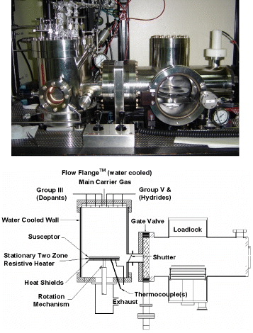
Figure 1 Photograph and schematic diagram of the Emcore D125 MOCVD growth chamber.
The samples used in this study were grown on quarters of 2-inch diameter (0001)-orientation (c-plane) sapphire substrates. During the growth, the chamber pressure was controlled at 100–300 Torr. Trimethylaluminum (TMAl), trimethylgallium (TMGa), trimethylindium (TMIn) and ammonia (NH 3) were used as aluminum, gallium, indium and nitrogen sources, respectively. Biscyclopentadienyl magnesium (CP 2 Mg) and disilane (Si 2 H 6) were used as the p-type and n-type doping sources, respectively.
Prior to growth, the substrates were cleaned by a H 2 SO 4:H 2 O 2 (3:1) solution for 10 min, then etched in 2% HF solution and rinsed in deionized water, followed by N 2 blow-drying. After loading, an in situ thermal cleaning procedure was applied to the sapphire substrates for 10 min at 1080 °C under H 2 ambient to remove native oxide from the substrate surfaces. After cooling down from the thermal cleaning step, a GaN buffer layer of about 30 nm was deposited at 525 °C. After that, the temperature was elevated to 1020 °C to grow a 1 μm thick GaN layer and then a 1 μm thick Si-doped, n-type GaN layer. The substrate temperature was subsequently ramped down to grow the InGaN well layer at 715 °C and grow the GaN barrier layer at 840 °C. The InGaN/GaN MQW active region consists of three pairs of 3 nm thick In 0.4 Ga 0.6 N-well layers and 10 nm thick GaN-barrier layers. After the growth of the active region, a 30 nm GaN cap layer was grown on the multi-quantum wells and the substrate temperature was elevated to 727 °C to grow a 250 nm thick Mg-doped p-type GaN layer. We grew LED structures on the sapphire substrate, as shown in figure 2.
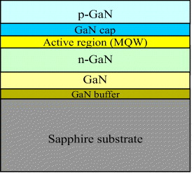
Figure 2 Schematic drawing of the sample structure.
In order to increase the indium incorporation rate, nitrogen was used as the carrier gas when we grew the InGaN MQW active regions. On the other hand, hydrogen was used as the carrier gas when we grew other parts of the samples. The as-grown LED structure samples were annealed at 730 °C for 30 min in N 2 ambient to activate the Mg-doped p-type GaN layers. The growth was monitored in situ by reflectometer measurements at a laser wavelength of 635 nm.
2.2. Fabrication of InGaN/GaN MQW LED chips
In this study, we used an inductively coupled plasma (ICP) of Unanix SLR-7701-8R system for etching mesa for n-contact and E-beam Evaporator of Auto 306 system for metallization of the p–n electrode.
After the annealing, the surface of the as-grown samples was partially etched by this ICP system until the n-type GaN layer was exposed for n-type ohmic contact. The depth etch was 700 nm within 165 s. The conductivity of the p-type GaN is not good enough for current spread due to the low active efficiency of the Mg dopant. So, Ni/Au (5 nm/5 nm) contacts were subsequently evaporated onto the p-type GaN layer to serve as the semi-transparent metal ohmic contact to improve the holes current spread. Then a 200 nm Au contact was deposited on top of the semi-transparent layer to serve as the p electrode. On the other hand, Ti/Al/Ni/Au (10 nm/200 nm/30 nm/100 nm) contacts were deposited onto the exposed n-type GaN layer to serve as the n-type electrode. Figure 3 shows a schematic drawing of the sample structure.
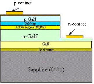
Figure 3 Structure of the fabricated blue LED chips.
The current–voltage (I–V) characteristics were measured at room temperature with an I–V Measurement System, while the luminous intensity and wavelength of the blue LED chips were measured with an LED chip tester.
Subsequently, the blue LED chips were fabricated on quarters of 2-inch diameter sapphire substrate. These LED chips were then further coated with suitable chemicals to produce white LED lamps. To convert the blue light emitting LED chips into white light emitting ones, a solution of yellow phosphor (Y 3 Al 5 O 12:Ce) [12–14] and epoxy resin was prepared, then coated on the surface of the blue LED chip. Depending on the concentration of the powder phosphor in the prepared coated solution, a cool white or warm white lighting from the LED lamps was obtained.
3. Results and discussion
LED chips were produced from quarters of 2-inch diameter of sapphire wafer and final blue chips with dimensions of 315×315 μm 2. Images of several LED chips are shown in figure 4(a), while figure 4(b) demonstrates the blue light, emitted from the fabricated chips.
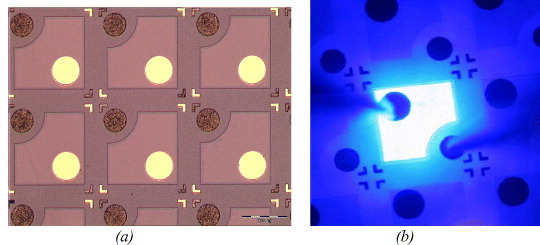
Figure 4 (a) Photograph of several LED chips and (b) blue light emitted from the fabricated LED chips, as measured by I–V measurement system (Agilent).
3.1. Current–voltage measurement
Figure 5 shows the current–voltage (I–V) characteristics of InGaN/GaN blue LED with the same chip size as a function of forward driving current. The results show that the turn-on voltage and contact resistance are about 4 V and 125 Ω, respectively. The forward voltage (VF) for the LED chips was 5.5 V at the forward injection current of 40 mA.
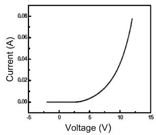
Figure 5 Current–voltage characteristic of the fabricated LED chips.
3.2. Electroluminescence measurement
Figure 6(a) shows the room temperature electroluminescence (EL) spectra of the InGaN MQW LED at an injection of 40 mA. A strong emission peak can be observed at the wavelength of 466.5 nm.
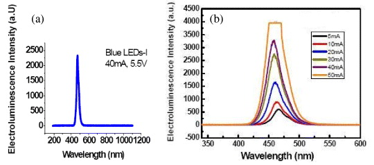
Figure 6 Room temperature electroluminescence measurement of the fabricated LED chips.
To evaluate the effective operation of fabricated InGaN/GaN blue LED chips, the electroluminescence measurements were performed at the forward injection currents of 5, 10, 20, 30, 40 and 50 mA. We found that the LED chips at 50 mA and above made the photodetector saturate, as shown in figure 6(b). The reduction in peak wavelength with higher injection current can be attributed to the piezoelectric field effect.
3.3. Luminous intensity measurement
The luminous intensity of the fabricated blue LED chips, measured by an LED chip tester, was approximately 80 millicandela (mcd) with a current of 20 mA. The wavelength of blue emitting light was about 450 nm. After coating the fabricated chips with the yellow phosphor (Y 3 Al 5 O 12:Ce) and epoxy resin, we obtained the white LED lamps (figure 7), and the power of the fabricated white LED lamps is about 40 lm W -1 at 20 mA current.
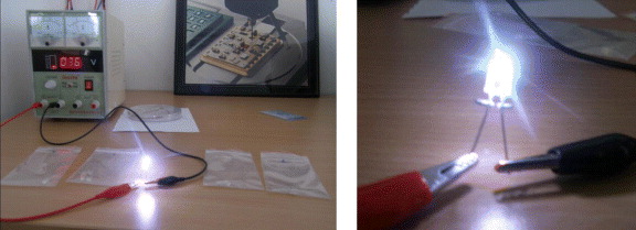
Figure 7 Emission of white light from the surface modified LED chips.
4. Conclusions
In this paper, MOCVD was successfully used to grow multilayers of nanometer thickness, high quality III-N films on a sapphire substrate for subsequent realization of LED devices. Then standard fabrication techniques of photolithography, metal deposition, lift-off, etching, etc, were utilized to realize LED chips of 315×315 μm 2 from the deposited sapphire wafer. The realized LED devices emitted blue light with a luminous intensity of approximately 80 mcd, measured with a current of 20 mA. To obtain the white light LED device, the fabricated chips were coated with a solution of yellow phosphor (Y 3 Al 5 O 12:Ce) and epoxy resin. The power of the realized white LED lamp was about 40 lm W -1 at measured 20 mA current. The obtained results prove that both the blue and the white LED based lamps were successfully fabricated.
Acknowledgments
The authors appreciate the financial support of the Vietnam Ministry of Science and Technology (MOST) and the Vietnam Academy of Science and Technology (VAST). We also would like to thank the staff members of the Centre for Optoelectronics (COE) and the Institute of Materials Research and Engineering (IMRE)—National University of Singapore (NUS), Singapore, for their technical support.