
Abstract
The passive RFID tag with an added sensing function is of interest to many applications. In particular, applications where RFID tagging is already considered to be the next step, such as food items, are a specific target. This paper demonstrates a flexible RFID tag sensor fabricated using a low cost technique with an added zero-cost sensing function. It is more specifically applied to the sensing of degradable food, in particular beef meat in our demonstrated example. To reach this, the antenna is designed in such a way to be sensitive to the variation of the dielectric permittivity of the meat over time. The design of the sensing tag as well as its fabrication process are described. The fabrication involves inkjet printing of a silver nanoparticle based ink on a commercial low cost PET film to create a seed layer. It is followed by a copper electrodeposition step on top of the silver pattern to complete the tag to obtain the desired thickness and conductivity of the tag antenna. The results of the electrical tests showed that with the inkjet printing–electrodeposition combination it is possible to produce flexible electrically conductive patterns for practical RFID applications. The tag was then tested in close-to-real-world conditions and it is demonstrated that it can provide a sensing function to detect the consumption limit of the packaged beef.
Export citation and abstract BibTeX RIS

Original content from this work may be used under the terms of the Creative Commons Attribution 3.0 licence. Any further distribution of this work must maintain attribution to the author(s) and the title of the work, journal citation and DOI.
1. Introduction
Radio frequency identification (RFID) technology is a very important development at the crossroads of several technology streams of the past decade. It is especially clear when considering passive RFID ultra high frequency (UHF) tags, i.e. tags without onboard battery but readable at long distance beyond 5 m. In most cases they need to be fabricated on flexible substrates, with low cost processes while being able to work in a rough environment.
The application range of UHF RFID technology is very wide [1]. Some major applications currently based on RFID technology include the retail supply chain [2], the military supply chain, pharmaceutical tracking and management, access control, sensing and metering, parcel and document tracking, automatic payment solutions and vehicle identification. The adoption rate of RFID technology is, however, considered slow as there are many constraints associated with the lack of embedded power source on the tag, and the difficulty to adapt the technology to various environments while ensuring a perfect readability of the tags. This pushes developments of RFID UHF tags which are functional on metal parts [3] or liquid containers [4]. The general trend in this respect is to design such tags to be readable in the widest possible cases, i.e. to be as insensitive as possible to their environment.
The problem however can be reversed to provide the RFID tag with a sensor function at 'zero cost'. In fact, the sensitivity of an RFID tag to its environment can be put into use by designing it in such a way as to have the impedance matching between the antenna and the integrated circuit changing with the surrounding dielectric permittivity [5]. This is the principle on which we have designed the RFID sensor in this work.
Another aspect of the slow uptake of the technology is the cost of the individual tag. For most applications, the added value of individual item identification is only acceptable at very low cost for the final user. Nevertheless, progress is constantly being made to develop low cost RFID tags. Different printing techniques such as inkjet printing, gravure printing, screen and flexographic printing have been used to fabricate electronic circuits and radio frequency identification (RFID) tags [6–8]. All of these techniques allow for the same order of magnitude in resolution, between 10 and 30 μm. Among them, inkjet is advantageous due to its maskless nature [9].
In this paper we present a prototype of low cost RFID sensor to detect the shelf life of meat products. We describe its fabrication using low cost techniques and demonstrate its functioning in real-world conditions.
2. RFID tag design
2.1. Principle
The literature indicates that the dielectric permittivity of food evolves as a function of time under standard storage conditions [10]. When an RFID tag is in close proximity with the food, its antenna impedance depends on the dielectric permittivity of the food. Starting from the impedance matching between the antenna and the tag's integrated circuit defining the maximum reading distance, a change in the food dielectric permittivity will modify the read-range due to the detuning between the chip and the antenna. This forms a way to detect the change of dielectric permittivity of the food.
This defines the way the present RFID tag is designed. We aim at applying the targeted sensor to packaged beef in supermarket storage conditions. First, the meat dielectric permittivity is measured over time (see next section). Then this set of data is used in simulation software to obtain the read range of specifically designed tags and obtain the largest difference in read range between fresh and contaminated meat.
2.2. Meat dielectric permittivity measurement
The beef sample to be measured is stored under supermarket conditions (temperature of 5 ± 1 °C and humidity of 50 ± 5%). The beef used is from a supermarket (METRO®, France).
The dielectric permittivity is measured every 12 h during 10 consecutive days. The measurement is done at 868 MHz (ETSI regulation of UHF RFID, valid in Vietnam) using an HP85070B coaxial probe from Agilent® [11]. In parallel, the pH of the meat was measured using a pH-meter (PH-506). Both probes are entering the meat over 5 mm in order to ensure a good reproducibility of the measurement.
Both the dielectric permittivity and the pH were measured at 4 locations, different for both measurements. The values are the result of an average of 3 measurement samples at each location figure 1.
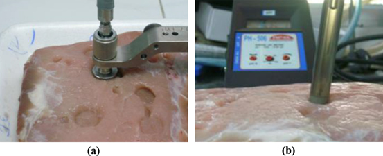
Figure 1. Dielectric permittivity (a) and pH (b) measurements.
Download figure:
Standard image High-resolution imageThe results for pH are shown in figure 2. The pH steadily increases up to 6.2 up to 48 h, and then marks a plateau until around 120 h and further increases continuously up to 192 h before its behavior changes again to be non-monotonous.
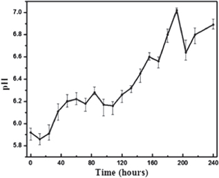
Figure 2. Beef pH versus time.
Download figure:
Standard image High-resolution imageThe dielectric permittivity and loss factor of the beef sample present an interesting behavior (figure 3). First of all we notice that there is a rather strong noise in the measurement results, probably due to the difficulty to obtain perfect reproducibility from one sampling to the other over 2 measurement periods. Nevertheless out of this, a general trend seems to emerge. First of all both dielectric permittivity and loss factor present a rather constant baseline for most of the time. The dielectric permittivity baseline is in between 57 and 59 while the loss factor comprises between 20 and 22. Then at 120 h for both, there is a peak which reaches 62 and 24, respectively. The peak for the dielectric permittivity is narrower than for the loss factor, the latter spreading from 96 to 120 h.

Figure 3. Beef dielectric permittivity (a) and loss factor (b).
Download figure:
Standard image High-resolution imageThe standard on pH for meat freshness [12] indicates that 6.2 is the accepted limit. From figure 2, it is not so direct to determine an exact threshold in terms of time as the plateau of pH near 6.2 is spread over a long time. It is obviously also not practical to measure the pH of the meat when packaged under storage conditions. In contrast, the dielectric permittivity presents a localized maximum in time which can advantageously be used for sensing purpose.
At present there is no further data in the literature on which an understanding of the observed dielectric permittivity behavior of the beef meat can be built. Nevertheless, an equivalent behavior was measured on pork meat in the same conditions. Thus, despite an absence of biophysical supporting explanation, we show that the dielectric permittivity evolution over time of the beef meat can be used for contamination sensing purpose (section 4).
The dielectric permittivity of the fresh beef is 56.8 + 22.6i (at the start) and 61.8 + 24.0i at the state of contamination (at 120 h). The different values of the permittivity between the two states (fresh and contaminated) are subsequently included in the simulation model for the design of the sensor tags to take into account the effect of beef state on the read range.
2.3. Tag structure
The tag is based on the AK3 Tagsys loop consisting in an integrated circuit connected to an inductive loop on a polyethylene terephthalate (PET) substrate. It is coupled to a meander antenna separately fabricated on a PET substrate, as shown in figure 4.

Figure 4. RFID tag structure.
Download figure:
Standard image High-resolution imageThe advantage of such a structure is the improved repeatability of the tag properties as the Tagsys loop is manufactured in an industrial environment. The antenna is thus separately designed and fabricated to adapt to the specific problem of the beef meat quality sensing.
The different thicknesses and materials properties of the parts of the tag are taken into account in the simulation model implemented in CST Microwave Studio.
2.4. Results
Several structures were tested in a search for the highest read range in the permittivity range of interest, i.e. 58 to 62 (figure 5). The most sensitive structure is presented in figure 5. It displays a computed read range variation of 20 cm over the dielectric permittivity range of interest.

Figure 5. Read range as a function of the dielectric permittivity and corresponding antenna structure.
Download figure:
Standard image High-resolution image3. RFID tag fabrication
The tag antenna is patterned by inkjet printing to act as seed tracks for the thickening by copper electrodeposition. This way it is possible to combine the simplicity of maskless patterning of the inkjet printing with the low cost metal deposition of electroplating.
3.1. Antenna patterning
A dimatix materials printer DMP-2800 (Fujifilm Dimatix, USA) is used with 16 nozzle cartridges of 10-picoliter drop volume (DMCLCP-11610). RFID antennas were printed using commercial silver ink (U5603, SunChemical, USA). This ink is a solution of silver nanoparticle at 20 wt%. It consists of nanoparticles with a narrow size distribution with an average diameter of 30 nm.
The antenna is printed on a commercial 80 μm thick PET substrate. It is carefully cleaned using a sequence of acetone, ethanol and deionized water baths followed by dry nitrogen drying.
The printing parameters were optimized first. These parameters include the distance between the print head and the substrate, the temperature of the substrate, the drop spacing and the waveform profile to actuate the nozzle. During the printing process, the distance between the print head and the substrate was maintained at 1 mm and the substrate was heated and maintained at 60 °C. The optimal values of droplet spacing in both X and Y directions were found to be 20 μm for 10 pl droplets. At this drop spacing the formed films keep well-defined shape while being thick enough to properly conduct electrical current for the subsequent electrodeposition. These optimized parameters were used for all the printing trials.
A very common cause of nozzle failure originates in entrained air bubbles during the printing process. An air bubble will influence the acoustics of the channel inside the print head which leads to modified drop formation process and results in nozzles failure. The ink can contain a large amount of dissolved gas which will create small bubbles under the influence of the drop formation process. This air can originate from the ink manufacturing process or from failure in the ink supply system [13]. This necessitates carefully removing bubbles in ink, which in our case is done using a specific degasing bench.
To ensure a well-defined antenna, it is necessary to stabilize the printing process so as to remove satellite droplets [14]. Satellite droplet formation is one of the most troublesome issues. When the waveform used for printing is not perfectly adjusted, the drop has a long tail after it leaves the nozzle. This long tail separates from the primary droplet and breaks into small satellite droplets. After the primary droplet hits the desired location, the satellite droplets arrive on the substrate fractions of a second later and land behind the main droplet.
Reducing voltage [15], modifying the waveform [16] and removing gas from ink improved the printing quality to result in significant reduction in nozzle failure and the improvement of dot circularity, as shown in figures 3 and 4. The droplet has good uniformity with no satellite and bubble occurrences (figure 6).
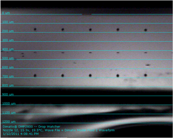
Figure 6. Adjacent droplets under good jetting conditions.
Download figure:
Standard image High-resolution imageOnce the antenna patterns are formed, it is necessary to stabilize the obtained film by curing it. The PET substrate has a low temperature of glass transition. As a consequence, the annealing of the printed silver film should happen at low temperature. To check the effect of the annealing temperature on the consolidation of the film, lines with different drop spacing, from 5 to 45 μm, were annealed for 2 h at 100 °C and 150 °C (the highest temperature stood by PET in conventional oven). Their 3D shapes were measured using a confocal microscope (Sensoscan, Sensofar, Spain). Figure 7 presents the cross section area of both series.

Figure 7. Cross section of printed lines at different drop spacing at 100 °C and 150 °C.
Download figure:
Standard image High-resolution imageIt is clearly visible that the increased temperature does not help here to consolidate the nanoparticles, which means that the best densification of the printed antenna is reached at low temperature.
3.2. Antenna thickness adjustment
The printed Ag nanoparticles were meant to be as a conductive seed layer for subsequent copper deposition. The plating solution is a standard low speed copper sulfate based solution at 45 g l−1. The Surtec additives (brightener, leveler and make-up solution) were added as indicated by the manufacturer (Surtec, Germany). One 10 cm wide anode is used facing the substrate at about 10 cm distance. The bath is kept at room temperature and aerated during the deposition. The plating current density is set at 0.1 A dm−2 and the plating current is computed from the area of the antennas to be plated, this being obtained from the design software. The metal thickness is then controlled through the plating time. After the samples are removed from the plating bath, they were thoroughly rinsed with deionized water to remove loose copper and plating solution. They were then dried by blowing nitrogen.
The copper thickness is measured by a Dektak6M mechanical profilometer (Veeco, USA). The sheet resistance of copper deposit is measured by a 4-point prober. Figure 8 shows that the copper thickness evolves linearly with time which reflects that the electrodeposition process takes place in stable conditions at a rate of 2.1 nm s−1.
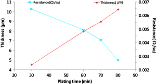
Figure 8. Evolution of the copper film thickness and its sheet resistance with plating time.
Download figure:
Standard image High-resolution imageThe sheet resistance decreases in a nonlinear fashion as the film thickens. The resistivity of the film is 3 μΩ cm at 4.5 μm down to 2.5 μΩ cm at 10 μm. This is usually a consequence of a denser film during the plating process. Even though not as low as the bulk copper resistivity, this range is enough for the purpose of designing an RFID tag. All the fabricated tags were with 10 μm thick antennas.
Figure 9 shows the final RFID tag with the specifically designed antenna and the mounted AK3 Tagsys loop, accurately positioned thanks to identical markers both on the antenna and the loop.
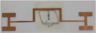
Figure 9. Final tag: fabricated antenna with the AK3 Tagsys loop placed on it.
Download figure:
Standard image High-resolution image4. Measurement in real conditions
The fabricated RFID tag sensor was placed on a packaged beef sample. The read range was measured in conditions close to real world on a bench presented in figure 10. As for the measurements on the beef sample presented in section 2, the measurements were performed every 12 h from the fresh state. They were performed over 7 consecutive days.
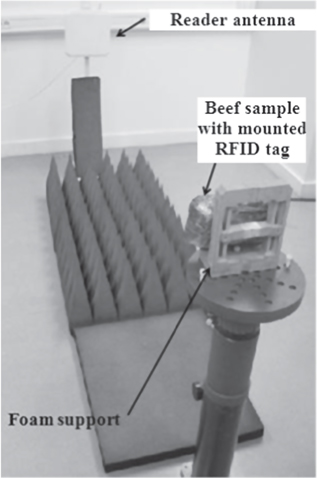
Figure 10. Measurement bench for read range determination in close to real-world conditions.
Download figure:
Standard image High-resolution imageThe read range variation over time is shown in figure 11 for two tags. This demonstrates the reproducibility of the fabrication process flow at laboratory scale. It is interesting to note that the largest read range difference occurs between 30 and 90 h, instead of the expected 120 h from the experimental data on dielectric permittivity. Another interesting characteristic is that the read range variation is 30 cm, higher than the original design.

Figure 11. Read range measurement.
Download figure:
Standard image High-resolution image
These observed differences with the simulation come from the inability of the simulation to perfectly render the real conditions. In reality, the physical dimensions of the packaged beef sample are larger than in the simulation. The detailed conditions of humidity and temperature are also not easy to stabilize and small variations can easily induce effects on the conditions of measurement of the tag mounted on the beef sample.
5. Conclusion
In this work we demonstrated for the first time the possibility to use a specifically designed UHF RFID tag as a sensor for food product state of degradation. We could make use of the change of dielectric permittivity in the packaged food to influence the read range of the tag mounted on it. This constitutes an interesting 'zero cost' sensor as the tagged product can have its freshness state checked at the same time it is tracked.
Among interesting directions for our future research, we think that the read range needs to be improved. This can be done in particular by making use of a lower power integrated circuit. The current one has an activation power of −15 dBm while state-of-the-art RFID integrated circuits present a lower power. Work can also be done on the reader side to automate the reading process and design the system to be placed in a supermarket environment.
Acknowledgments
The authors highly appreciate the financial support of the Ministry of Sciences and Technology of Vietnam. The authors are grateful to Tagsys Company for providing the AKtag RFID chips.