
Abstract
This paper describes the attachment of conjugated oligomers onto electrode surface through the reduction of diazonium compounds. In this connection some properties of conjugated oligomers and of layers grafted through diazonium electroreduction will first be briefly presented. The electrochemical behavior of conjugated oligomers grafted on a surface using diazonium electroreduction will then be discussed.
Export citation and abstract BibTeX RIS

Content from this work may be used under the terms of the Creative Commons Attribution 3.0 licence. Any further distribution of this work must maintain attribution to the author(s) and the title of the work, journal citation and DOI.
1. Conjugated oligomers and polymers
Since their discovery, conjugated oligomers (COs) and conjugated polymers (CPs) have been widely studied for scientific and technological issues. Figure 1 recalls the main classes of CP based materials. Some of them, such as poly-p-phenylene, polyvinylenephenylene are based on carbon aromatic moieties, whereas polypyrrole, polythiophene, polyaniline and various derivatives are based on heteroaromatic monomers.

Figure 1. Various types of conjugated oligomers and polymers. 1—Poly-p-phenylene (PPP); 2—poly(phenylenevinylene)(PPV); 3—polypyrrole (PPy), polythiophene (PTh); 4—polyaniline (PANI).
Download figure:
Standard image High-resolution imageOne of the most important properties of COs and CPs is their ability to transport charge at the molecular level along the backbone of alternating simple and double carbon–carbon bounds. This property is less attenuated with distance than in saturated molecular systems or through space. As a consequence, COs and CPs have been proposed as building blocks for molecular electronic devices and many experimental [1] and theoretical studies [2] have been devoted to understanding their charge transport properties in various configurations from thin layer systems to single molecule devices [3]. Another crucial property is their ability to switch upon chemical, electrochemical or electrical doping, between two states with different electron transport properties. Such processes lead to CP charging and this corresponds to an electrochemical oxidation in the case of p-doping (polymeric chains are positively charged) and to a reduction in the case of n-doping. CO and CP are thus electroactive species and redox potentials for doping/dedoping processes have been studied in detail. They depend both on the number of monomer units (n) in the oligomeric chain, on the type of monomer and on the number of defect along the chain. A linear dependence of the redox potential versus the inverse of the number of monomer unit (1/n) has been experimentally observed (for short oligomers). As examples the redox potential of oligoparaphenylene and oligothiophene of various length are given below [2].
.
| Oligoparaphenylenes | Oligothiophene | |
|---|---|---|
| n-doping | E0(n)=−1.52 | E0(n)=−1.95 |
| ×1/n−1.90 | ×1/n−1.42 | |
| p-doping | E0(n)=1.56 | E0(n)=1.80 |
| ×1/n+1.08 | ×1/n+0.35 |
Upon doping, the conductance of CP film varies considerably (σdc ∼ 10−8 S cm−1 in the undoped state and σdc ∼ 100 S cm−1 when doped) [1]. For electroneutrality reasons doping is accompanied with ion insertion easily detected using x-ray photoelectron spectroscopy (XPS) spectroscopy and by a quinoidic deformation with distinct signature in IR or Raman spectroscopies [2].
Electrochemical switching of CO and CP has proved to be an easy means of controlling the properties of grafted molecules [4] and of metallic nanoparticles [5]. It is used in redox-gated single-molecule devices [6]. Electrical doping of COs is the basis of their increasing use in low-cost plastic and printable electronics as field-effect transistors. This switching property is also the basis of Aviram proposal in which a single molecule consisting of two oligothiophene is used for processing information at the molecular level [5]. Despite its visionary aspect, such a system suffers severe drawbacks, and grafting the two oligothiophenes on electrodes is absolutely necessary for long-term stability.
Many other scientific domains use CP and CO as thin films or coatings [1, 2]. Most applications rely on electrochemical properties: batteries, electrolytic capacitors and electrochromic devices are based on their electrochemical switching properties. Other applications are linked to the conductive state of such materials. Poly(ethylene dioxythiophene) (PEDOT), a soluble polythiophene derivative developed by Bayer AG and initially used as antistatic coatings can be easily deposited using spin- and dip-coating techniques on any kind of substrate, including flexible ones. It is now widely used as a hole injection layer in numerous organic electronic devices. Applications as anticorrosion layers also represent an important part of polymer production, and delamination of the coating at the CP/metal interface is an identified failure process of anticorrosion protection [7]. New researches explore new frontiers and combining CP nanostructuration with dynamic switching properties has been proposed as the basis of smart surfaces for tuning anticorrosion and biofouling properties or hydrophobicity and wettability of the coatings [8]. For those applications, CO and CP are deposited using various techniques, either from solution (dip-coating, self-assembly) or the vapor phase, or by electrochemical oxidation of a monomer. In such cases, the bond between the substrate and the deposited oligomers is not covalent and the interface is often ill defined, which may strongly limit the lifetime of the coatings.
In other words, monolayer or ultrathin layers based on conjugated oligomers, with a well-defined metal/oligomer interface, thanks to a covalent bond, and retaining reversible on/off switching capabilities controlled by the redox state of the oligomer, are of interest for single or large-scale molecular electronic devices, for smart surfaces and for most applications where conjugated oligomers and polymers are used.
2. Surface grafting based on electroreduction of diazonium salts
Downard [9] and Podvorica and Pinson [10] recently reviewed the modification of electrodes using aryl diazonium salts. The basic reaction mechanism was first described for the modification of carbon electrodes by Pinson and co-workers [11] and is depicted in figure 2. A radical is generated at low reduction potentials and reacts with the underlying electrode to form a covalent C–C bond with the substrate (carbon surface, gold, copper). This bond is significantly stronger and more stable than the gold–thiol bond. Figure 3 shows the current–voltage characteristic (CV) corresponding to the grafting of 4-nitrobenzene diazonium tetrafluoroborate on a glassy carbon (GC) electrode. A broad irreversible wave can be observed in the first cycle. On the second scan, the wave disappears nearly completely which is indicative of the blocking of the surface by the grafted organic groups.
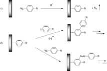
Figure 2. Reaction mechanism for the electroreduction of aryl diazonium salts to electrode surfaces and the main side reactions.
Download figure:
Standard image High-resolution image
Figure 3. Typical electrochemical response of an electrode during diazonium electroreduction first (a) and second (b) scans. (c) CV of the same GC electrode in acetonitrile (ACN) + 0.1 M NBu4BF4. From [10].
Download figure:
Standard image High-resolution imageThe reaction depicted in figure 2 is only the dominant reaction of the grafting process, since side reactions do also occur. Figure 2 also shows the two most significant side reactions: (i) radical attack at the ortho or the para (if sterically free) positions of a surface bound aryl group [10], which creates the possibility of multilayers consisting of conjugated oligomers that can be more easily doped than monolayers even though they will be obtained by the same diazonium precursor; (ii) bonding to the surface without loss of the diazonium group [12].
Because of the low reduction potential required for grafting and the lack of organization induced by multilayer deposition, the generated organic layer is, in most cases, insulating at the potential used during grafting and the process self-terminates for thicknesses where tunneling current across an insulating barrier vanishes. As a consequence, films obtained are usually ultrathin with thicknesses between 5 and 10 nm.
Outer-sphere redox probes in solution are widely used to probe the charge transfer properties of such ultrathin aryl modified layers deposited on the electrode. They generally display four types of voltammetric responses.
- No current observed in the potential window where the redox probe is electroactive on a bare electrode which indicates the presence of a homogeneous insulating layer at the surface.
- A stationary current far below that observed on a bare electrode which indicates that the surface is composed of pinholes/microelectrodes which do not communicate between them [13].
- Increase of the peak potential separation (ΔEp) along with a decrease of the corresponding peak current (Ip) which indicated a partially blocking effect of the electrode surface. This can be explained either by the presence of a grafted layer which decreases the apparent electron transfer kinetics, or by the presence of many pinholes/small electrodes which communicate between them [13].
- Behavior (current, peak potential position and separation) similar to that observed for a bare electrode as a consequence of an unsuccessful grafting which left the surface unchanged, or because the deposited layer is conductive.
Another technique to characterize such layers is to deposit a top electrode on the grafted organic layer and to generate large-area metal/molecule/metal junctions and to measure the charge transport properties (I/V characteristics) of such devices.
3. Deposition of oligo-phenylthiophene or oligothiophene mono- and multilayers through diazonium electroreduction
The electroreduction of in situ formed 1-(2-bisthienyl)-4- aminobenzene (BTB) and 1-(2-thienyl)-4-aminobenzene (TB) diazonium salt derivatives yielded ultrathin film (thickness in between 5 and 20 nm) strongly attached to the surface (figure 4). Such films are electroactive at potential close to 0.5 V and 0.7/SCE (saturated calomed electrode), respectively [14]. Note also that the layers are composed of short oligo(BTB) or oligo(TB) grafted on the surface despite the fact that they are labeled as BTB and TB, respectively.

Figure 4. Amino aromatic compounds bearing one or two thiophene units, their corresponding diazonium salts and their grafting of an electrode. Reprinted with permission from [14]. Copyright 2007, American Chemical Society.
Download figure:
Standard image High-resolution imageThe electrochemical response of several redox probes (decamethyl ferrocene (DmFc), ferrocene (Fc), aminodiphenylamine (ADPA) and thianthrene (Th)) on GC surfaces modified with BTB and TB were reported.
Unique electrochemical responses were obtained [14, 15].
- For DmFc, Fc and ADPA first wave, that is redox probes with redox potential lower than that of the layer, no current was observed on the modified electrodes in the classical potential range for such probes on bare electrodes. However, the current quickly increases at higher potentials, and irreversible oxidation waves are recorded. As a consequence the layer induces a 'diode-like behavior' on the electrochemical response of such probes. The oxidative peaks of the probe can be tuned according to the nature of the organic layer. Ferrocene anodic peak potential is centered at 0.53 V on BTB, whereas it is at 0.73 V when measured on a TB layer.
- For thianthrene, ADPA second wave, that is redox probe with redox potential above that of the layer, in contrast, a reversible response very similar to that obtained on bare GC was recorded (figure 5).
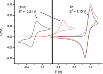
Figure 5. CVs of a bare GC (black) and BTB-modified (red) electrodes for DmFc + /DmFc and Th + /Th in an ACN + 10−3 M redox probe +0.1 M LiClO4 solution. Scan rate: 0.1 V s−1. Reprinted with permission from [15]. Copyright 2008, American Chemical Society.
Download figure:
Standard image High-resolution imageSuch behaviors were interpreted as due to a fast conductance switch (within the time range investigated) of the layer induced by hole injection (p-doping) in the grafted material.
An anodic potential shift is observed for DmFc, Fc and the first oxidation of ADPA redox couples because at their respective redox potential the layer is insulating and must be p-doped in order to allow charge transfer. No cathodic peaks are observed for those probes during the reverse scan because the layer has switched back to its insulating state before reaching the reduction potential of the probe. In contrast, when the probe redox potential is in the range where a large amount of charge has been already injected into the organic layer, the layer is conductive and current can flow in both directions. As a consequence, the organic layer appears to be completely 'transparent' for these redox probes.
As a consequence, oligothiophene-like materials, retaining on/off switching properties of conjugated oligomers, while being covalently grafted on the electrode were successfully obtained.
A further extension of this p-doped oligothiophene based grafted layer was reported using a new diazonium salt, derived from a heteroaromatic compound, 2-aminoterthiophene [16]. This compound was the first example describing the electrochemical reduction of diazonium salt without phenyl ring. Ultrathin deposit terthiophene or oligothiophene layers were thus generated. The grafted layer was electroactive with one electrochemical signal similar to that observed when oligothiophene is solubilized in 0.1 M LiClO4 in acetonitrile (ACN) and oxidized on a bare electrode. This electrochemical signal corresponded to a total charge of 1.75 × 10⁻⁹ mol cm−2 deposited electroactive molecules after sonication. The surface coverage found here clearly indicated that the GC electrode is modified with a few molecular layers rather than with a thick film of oligothiophenes. Much alike BTB, this layer was shown to undergo a similar conductance switch upon p doping of the oligothiophene layer. This was nicely illustrated by grafting such layers on Pt ultramicroelectrode (UME) using several redox probes with redox potential lower (DmFc, Fc) or above that of the layer (Th) and using such switchable ultramicroelectrode in scanning electrochemical microscopy (SECM) experiments.
4. Host–guest complexation: a convenient route for the electroreduction of diazonium salts in aqueous media and the formation of composite materials and mixed layers
Diazonium salts are not always water-soluble and, therefore, they are frequently electroreduced in acetonitrile, which may be a severe drawback for environmentally friendly industrial processes. However, by using host–guest complexation, the solubilization of hydrophobic species in aqueous media is possible. BTB-modified electrodes generated in water/cyclodextrin (β-CD) were obtained using this strategy and the resulting organic electrodes exhibit the same conductance switch as those obtained in ACN. Such electrodes consist of grafted BTB molecules covering part of the bare electrode separated by β-CD molecules or domains of β-CD, incorporated in the layer. The electrochemical responses of several redox probes on these electrodes are similar to that obtained on a compact BTB layer which is compatible with the idea that each BTB wire acts as a molecular microelectrode. Cyclodextrin can be removed from the electrode using an adequate procedure (figure 6). This process appears to be partially reversible and can be used to control the electrochemical response of the electrode toward several redox probes in water [17].

Figure 6. Host–guest strategy to graft BTB/β − CD composite material and BTB/NP mixed layer in a two-step grafting procedure, Reprinted with permission from [17, 18]. Copyright 2010 and 2012, American Chemical Society.
Download figure:
Standard image High-resolution imageAn extension of this process was realized in order to generate mixed layer based on two different diazonium salts [18]. The strategy adopted is based on two successive electrochemical reduction of diazonium salts. First, BTB diazonium salt is reduced using host/guest complexation in a water/β-CD solution. The cyclodextrin trapped in the film is then removed from the surface leaving pinholes. Following this, nitrophenyl (NP) diazonium is reduced to graft a second component. Electrochemical study shows that upon grafting, NP moieties are grafted predominately in the empty spaces generated by β-CD desorption (figure 7). An exciting and unique result is that, after grafting an insulating material (NP moities) in between the electroactive BTB moities, the BTB/NP layer recovers the diode-like behavior (observed for a pure BTB layer but lost when pinholes are created), associated to the semiconducting properties and the conductance switch of the grafted BTB. Besides this approach, which leads to ultrathin mixed organic layers covalently attached to the surface, may constitute a very interesting route for the generation of novel electroactive multifunctional coatings. Such dilution may compete with and complement the well-known mixed alkyl thiols/gold self-assembled monolayers (SAM) coatings in many applications.
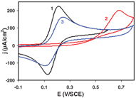
Figure 7. Cyclic voltammograms in 1 mM FcMeOH + 0.1 M LiClO4 in water on a bare carbon electrode (1) on a BTB/β-CD before (2) and after β-CD desorption (3). Scan rate: 100 mV s−1. Reprinted with permission from [17, 18]. Copyright 2010 and 2012, American Chemical Society.
Download figure:
Standard image High-resolution image5. Large-area molecular electronic devices using electrografted conductive oligomers
Such layers based on oligothiophene oligomers covalently grafted on gold or various substrates are very robust and may be suitable in molecular electronic devices fabrication. We have thus, in collaboration with Professor Lafarge, from the laboratoire des Matériaux et Phenomènes Quantiques de l'Université Paris Diderot, generated molecular junctions with the combined use of electrochemistry and conventional complementary metal–oxide–semiconductor (CMOS) tools. They consist of a 5–10 nm thick layer of oligo(BTB) between two gold electrodes (figures 8 and 9). The BTB layer is first grafted onto the bottom electrode using diazonium electroreduction. The top contact is obtained by direct electron-beam evaporation on the molecular layers through masks defined by electron-beam lithography which clearly shows that the electroreduction process yields to a stable and robust gold/oligomer interface (such direct top electrode deposition is not possible on SAM based monolayers) [19].
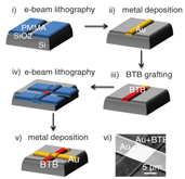
Figure 8. Schematic diagram of the different steps of the fabrication process of metal/molecule/metal junctions, Reprinted with permission from [19]. Copyright 2012, American Chemical Society. (i) e-beam lithography, (ii) metal deposition, (iii) BTB grafting, (iv) e-beam lithography, (v) metal deposition, (vi) SEM image of the device.
Download figure:
Standard image High-resolution image
Figure 9. Schematic representation of oligo(BTB) layer between the two electrodes, Reprinted with permission from [19]. Copyright 2012, American Chemical Society.
Download figure:
Standard image High-resolution image
Transport mechanisms across such easily p-dopable layers were investigated by analysis of current density/voltage (J–V) curves. Application of a tunneling model leads to transport parameters (thickness ≈ 2.4 nm) not consistent with the molecular thickness measured using atomic force microscopy (AFM) (≈ 7 nm). Furthermore, for these 5–10 nm thick layers, asymmetric J–V curves are observed with current flowing more easily when the grafted electrode is positively polarized. In addition, the J–V experiments at two temperatures (4 and 300 K) show that thermal activation occurs for such polarization but is not observed when the bias is reversed. These results indicate that simple tunneling cannot describe charge transport in these junctions. As a consequence the analysis of the experimental results in term of 'organic electrode' and redox chemistry in the material was discussed.
Finally, we recently extended, in collaboration with Professor Lafarge, and Professor McCreery from the University of Alberta (Canada), such studies to a thickness range between 5 and 22 nm, and in doing so we bridged the gap between short-range tunneling in molecular junctions and activated hopping in bulk organic films [20]. Moreover, we greatly extended the distance range of charge transport in molecular electronic devices. Indeed, we observed three distinct transport mechanisms for 4.5–22 nm thick oligo(thiophene) layers between carbon contacts, with tunneling operative when d < 8 nm, hopping when d > 16 nm for high temperatures and low bias, and a third mechanism consistent with field-induced ionization of highest occupied molecular orbitals (HOMOs) or interface states to generate charge carriers when d = 8–22 nm.
6. Conclusion and outlook
Conductive polymers and ultrathin layers based on diazonium electroreduction, being initially developed separately, have now come to a mutual enrichment. The latter brings some control of the interface between metal and oligomers, the former adds to grafted ultrathin organic layers new properties based on conductance switch, charge transfer and charge transport properties.
Monolayer or ultrathin layers based on conjugated oligomers, with a well-defined metal/oligomer interface retaining reversible on/off switching capabilities controlled by the redox state of the oligomer have therefore been reported.
They are of interest for large-scale molecular or electronic devices where organic electrodes, microelectrodes and molecular electrodes are needed. They will probably be used shortly in single molecular devices. They are also of interest for smart materials based on conductive polymers and are likely to have an important impact in many applications where conducting polymers adhesion on a surface is an issue.