
Abstract
I review the major research activities of my groups at the National University of Information Technologies, Mechanics, and Optics (St Petersburg) and Nonlinear Physics Center (Canberra, Australia) in the field of electromagnetic metamaterials operating at microwave and optical frequencies.
Export citation and abstract BibTeX RIS

Content from this work may be used under the terms of the Creative Commons Attribution 3.0 licence. Any further distribution of this work must maintain attribution to the author(s) and the title of the work, journal citation and DOI.
1. Introduction
Metamaterials, artificial electromagnetic media achieved by structuring on the subwavelength scale, were initially suggested to create media with the negative refraction and explore the advantages of the so-called superlensing. Later metamaterials became a paradigm for engineering electromagnetic space and controlling propagation of waves through transformation optics and invisibility cloaking. The main research agenda during the last few years has shifted toward the study of active metamaterials with tunable and switchable characteristics and novel functionalities such as the control of spontaneous emission and enhancement of Purcell states. Many of these functionalities can be realized with the help of nonlinear metamaterials.
This paper aims to summarize the major research activities of my groups at the National University of Information Technologies, Mechanics, and Optics (St Petersburg) and Nonlinear Physics Center (Canberra, Australia) in the field of electromagnetic metamaterials operating at microwave and optical frequencies.
2. Metamaterials controlled with light
Electromagnetic metamaterials demonstrate many intriguing properties such as artificial magnetism at optical frequencies, negative refraction, enhanced chirality and optical activity. Metamaterials can find many useful applications, e.g. for super-resolution and transformation optics. The majority of the demonstrated metamaterials possess fixed properties, but currently, many efforts are being made to achieve tunability of the metamaterial properties, either externally or by employing their nonlinear response. At microwave frequencies, it is easy to design a tunable nonlinear meta-atom as a split-ring resonator (SRR) loaded with a varactor diode that operates in either bias-free or biased regimes and subsequently create a bulk nonlinear magnetic metamaterial allowing a power-induced control of the wave transmission. Moreover, such artificial nonlinear media allow the demonstration of many interesting phenomena accessible at low powers such as a nonlinear-optical mirror.
In our recent studies [1–3], we proposed an original approach for creating tunable electromagnetic metamaterials. We demonstrated experimentally that magnetic resonance of a split-ring resonator ('meta-atom' of a composite material) with a photodiode operated in photovoltaic mode can be tuned by changing the intensity of an external light source. Moreover, for two coupled resonators, we show that we can achieve light-induced switching between dark- and bright-mode responses [1].
We also examined the properties of split-ring resonators loaded by varactor diodes to which a dc voltage is supplied from photodiodes integrated into the same element [2]. It has been shown that the magnetic response of the ring resonator is shifted down in frequency with an increase in the illumination intensity. In addition, we studied the nonlinear response of the developed resonator under variation of the power of the exciting signal, and demonstrated experimentally that an increase in the power shifts the resonance response to a higher frequency. Figure 1 shows the topology of the light-controlled split-ring resonator and a sample of the metamaterial, together with the measured reflection coefficient for various illumination intensities. The proposed ring resonators were later used to develop a new type of metamaterials with a nonlinear response tunable by an external light source.

Figure 1. (a) Topology of the light-controlled split-ring resonator. (b) Photograph of the light-tunable metamaterial sample. (c) Experimentally measured reflection coefficient of the split-ring resonator for various illumination intensities [2].
Download figure:
Standard image High-resolution imageRecently, we suggested and demonstrated experimentally the concept of novel functional metamaterials whose properties are remotely controlled by illuminating the metamaterial with a pattern of visible light. In such metamaterials arbitrary gradients of the effective material parameters can be achieved simply by adjusting the profile of illumination. We fabricated such light-tunable microwave metamaterials and demonstrated their unique functionalities for reflection, shaping and focusing of electromagnetic waves [3].
To demonstrate the flexibility of the light-tunable metamaterial mirror, we employed inhomogeneous light illumination patterns. First, we applied such illumination that the resonant frequency of the SRRs changes linearly along the structure. At a given frequency of operation this corresponds to a linear gradient in the reflection phase, which leads to the reflected beam deviation, so that the angle of reflection is not equal to the angle of incidence. When the gradient of illumination changes sign we observe reflected beam steering by 11°, as shown in figure 2.
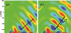
Figure 2. Experimentally measured real part of the of the scattered field distribution at f = 3.06 GHz for two different control light illumination patterns. The wave incident from the top-left corner reflects from the metamaterial mirror located at the bottom of the presented figures. (a) Light illumination decreases from left to right and (b) light illumination decreases from right to left. By changing illumination pattern the metamaterial mirror can steer the reflected beam by 11° [3].
Download figure:
Standard image High-resolution imageNext, we demonstrate that with a specifically crafted profile of illumination we may achieve focusing and defocusing by a planar structure. To obtain the corresponding spatial variation of the reflection phase, the illumination profile must resemble the parabolic phase distributions in concave and convex mirrors. Focusing and defocusing of the electromagnetic wave are clearly observed in our measurements.
Metamaterials are prominent for delivering exceptional opportunities they offer in tailoring macroscopic properties of materials through appropriate choice and arrangement of their structural elements. We believe that the approach suggested here will open new possibilities to implement tunability. Indeed, the ability to control the local material properties by applying light patterns may lead to unprecedented flexibility in confining, guiding or redirecting the flow of electromagnetic radiation. This will make it possible to fabricate dynamically tunable structures such as lenses and waveguides, as well as demonstrate the first fully reconfigurable cloaking device.
3. Nonlinear arrays of magnetic meta-atoms
Important building blocks of electromagnetic metamaterials are the split-ring resonators or other types of subwavelength resonant elements which are arranged in one-, two- or three-dimensional lattices. In general, the response of a metamaterial depends on the near-field interaction between the resonators within the system, and the metamaterials should be described as lattices of resonant elements by employing the techniques usually used in the analysis of photonic crystals and waveguide arrays [4–6].
Importantly, the effective interaction coefficients depend on the difference between electric and magnetic coefficients, which for experimentally realistic parameters may become comparable. By analyzing the near-field interaction between the SRRs, we found that the effective interaction coefficients are strongly different in x- and y-directions (as shown in figures 3(a) and (b)) and they can have different signs.

Figure 3. Electric and magnetic interaction coefficients (solid and dashed curves, respectively) as functions of the spacing between the ring centers for the fixed normalized frequency, when the rings are offset in (a) x direction, (b) y direction and (c) z direction. Insets show schematically corresponding ring positions [5].
Download figure:
Standard image High-resolution imageUsing these calculations of the near-field infarction, we analyzed the existence, stability and propagation of dissipative discrete localized modes in one-, two- and three-dimensional nonlinear lattices composed of weakly coupled SRRs excited by an external electromagnetic field. We employed the near- field interaction approach for describing quasi-static electric and magnetic interaction between the resonators, and demonstrated the crucial importance of the electric coupling, which can completely reverse the sign of the overall interaction between the resonators. We derive the effective nonlinear model and analyzed the properties of nonlinear localized modes excited in one-, two- and three-dimensional lattices.
In particular, we studied nonlinear magnetic domain walls (the so-called switching waves) separating two different states of nonlinear magnetization, and revealed the bistable dependence of the domain wall velocity on the external field, see figure 4. Then, we analyzed two-dimensional localized modes in nonlinear lattices of SRRs and demonstrate that larger domains may experience modulational instability and splitting.

Figure 4. (a) Dependence of the magnetization on the index n for S = 0.024. Solid-standing, and dashed-moving domain wall, corresponding to the top and bottom branches on the panel (c) in this figure. (b) Dependence of the velocity of the domain wall as a function of the external excitation S. Panel (c) shows a close up of the bistable region in panel (b), with arrows indicating directions of the jumps [5].
Download figure:
Standard image High-resolution imageIn addition, we demonstrated that nonlinear magnetic metamaterials comprised of a lattice of weakly coupled split-ring resonators driven by an external electromagnetic field may support entirely new classes of spatially localized modes-knotted solitons, which are stable self-localized dissipative structures in the form of closed knotted chains [6]. We demonstrated different topological types of stable knots for the subcritical coupling between resonators and instability-induced breaking of the chains for the supercritical coupling.
4. Wire metamaterials
Wire metamaterials represent a large class of artificial electromagnetic structures that can be regarded as optically dense arrays of aligned metal wires or rods embedded into dielectric matrices. Constitutive elements of wire metamaterials operating in the radio frequency range are usual millimeter or sub-millimeter-thick metal wires. For wire metamaterials operating in the THz range these elements are microwires, whereas nanowires or nanorods correspond to the infrared and visible range, see figure 5. The restriction of the optical density (or the low-frequency region of operation) separates wire metamaterials from metal–dielectric photonic crystals with wire inclusions. Metal wires offer a high optical contrast to the dielectric matrix, and this contrast of inclusions together with their geometry (inclusions are long and thin) determines the unusual properties of wire metamaterials. These properties allow us to classify such electromagnetic structures as metamaterials. Metamaterials are usually introduced as effectively homogeneous artificial materials with unusual (not realized for any natural medium) and useful electromagnetic properties.

Figure 5. Examples of wire media operating for (a) GHz, (b) THz and (c) visible frequency ranges. Examples (a) and (b) correspond to wire media employed for subwavelength imaging, whereas the example (c) is an array of free-standing nanorods [7].
Download figure:
Standard image High-resolution imageWe have studied various types of wire metamaterials and their specific properties [7–11] and also recently reviewed [10] both the physics and applications of such artificial electromagnetic materials composed of lattices of aligned metal rods embedded in a dielectric matrix. An important group of such metamaterials is a wire medium possessing extreme optical anisotropy. The study of wire metamaterials has a long history, however, most of their important and useful properties have been revealed and understood only recently, especially in the THz and optical frequency ranges where the wire media correspond to the lattices of microwires and nanowires, respectively. Another group of wire metamaterials are arrays and lattices of nanorods of noble metals whose unusual properties are driven by plasmonic resonances.
5. Metal–dielectric layered metamaterials
It is well accepted that the properties of optical metamaterials can be described by effective parameters derived under a broad assumption that the structural elements of a composite are much smaller than the wavelength. The effective medium is an important concept of the homogenization theory based on field averaging, and it provides a physical insight into the optical response of complex microstructured and nanostructured media, being also useful for different types of waves. However, it was already established that the effective medium models do not provide complete information, and they should be corrected in some cases, e.g. in the recently analyzed case of plasmonic nanorod metamaterials in the epsilon-near-zero regime, where the performance of such structures is affected by non-local response.
In several papers [12–14], we studied nanostructured metamaterials formed by a periodic layered structure (see the inset in figure 6), where metal and dielectric layers have different thicknesses. When the wavelength of radiation is much larger than the thickness of any layer, it is usually assumed that the effective medium approach is valid and the permittivity tensor for a uniaxial anisotropic medium.

Figure 6. Dispersion diagrams and the geometries of the periodic nanostructures composed of alternating metal and dielectric layers. Thicknesses of the layers are (a) d2 = 1.5d1 and (b) d1 = d2. Two dispersion branches corresponding to the actual structures are numbered by Roman numerals [12].
Download figure:
Standard image High-resolution imageHowever, we revealed that the dispersion properties of metal-dielectric periodic nanostructured metamaterials are dramatically affected by a non-local response due to excitation and coupling of surface plasmon polaritons at the metal–dielectric interfaces, so, in many cases, the effective medium approach fails to describe correctly the optical properties of such structures. The difference is dramatic, and it cannot be taken into account by small corrections. Furthermore, we found that the strength of optical non-locality can be engineered in a rather simple way, just changing a ratio between the thicknesses of metal and dielectric layers, so that the medium with equal layers demonstrates weak non-locality [12].
In addition to the effective medium analysis, we applied the standard transfer-matrix approach and analyzed, for definiteness, different structures formed by layers of metal and dielectric with various thickness ratios, but a fixed total period. The specific structures are illustrated schematically in the insets of figures 6(a) and (b). The dispersion diagrams for the two structures under consideration shown in figures 6(a) and (b) were computed using two approaches: the effective medium model (approximate approach) and the well-known classical dispersion relation for one-dimensional photonic crystals (exact description). Thus, we revealed a substantial difference between the results provided by these two approaches, even in the limit when the structure spacing is much smaller than the radiation wavelength.
We derived a model of a non-local effective medium for describing the effects of strong spatial dispersion in the multilayered metal–dielectric metamaterials [13, 14]. We obtained analytical expressions for the components of the effective permittivity tensor which depend on the wave vector and reveal that spatial dispersion effects exist in both directions across and along the layers.
Thus, we demonstrated that strong non-local effects predicted here can be observed as the splitting of the TM polarized wave at an interface between air and metal–dielectric nanostructured metamaterial into two waves with positive and negative refraction. Our results suggest the presence of strong spatial dispersion in many types of nanostructured materials and, in particular, they provide a proof that metal–dielectric nanostructures are inherently non-local metamaterials.
Surface waves appear in different problems of physics as a special type of waves localized near an interface separating two different media. In optics, linear electromagnetic surface waves are known to exist on metal surfaces at an interface separating homogeneous and periodic dielectric media as well as in layered structures containing thin metal films. The interest in the study of nonlinear electromagnetic surface waves has been renewed recently, and it was shown theoretically and experimentally that nonlinearity-induced self-trapping of light may become possible near the edge of a one-dimensional waveguide array leading to the formation of nonlinear Tamm states.
We have studied a novel type of Tamm states in nanostructured metal–dielectric metamaterials [15] and also presented a simplified analytical approach for the calculation of nonlinear dispersion of surface states in metal–dielectric nanostructures [16]. We showed that along with linear states such terminated structures support nonlinear states having a finite threshold power. We revealed that for the case of TM polarization two types of localized modes may exist even for the wavelengths much larger than the structure period. We also found that for the case of TM polarization up to four modes having the same frequency can be supported by the structure, i.e. the modes demonstrate multiple stability.
Profiles of the magnetic field for the surface states are depicted in figures 7(a)–(d). We note that for the case of TM polarization some surface states look like coupled surface plasmons at individual interfaces. We also see that for the case of ω = 4 eV there are neither linear nor nonlinear states in the structure with dielectric next to the nonlinear layer.
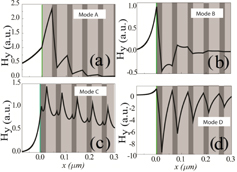
Figure 7. Profiles of the magnetic field amplitude for four different types of nonlinear Tamm states at the interface of metal–dielectric metamaterial in the case of TM-polarization [16].
Download figure:
Standard image High-resolution imageWe also studied surface modes at an interface separating two different layered metal–dielectric structures [17]. First, we analyzed a validity of the effective medium method and demonstrated that this approach allows one to predict only one surface mode with the dispersion that coincides with the dispersion of a surface plasmon at the boundary of two isotropic media. Next, we applied the transfer-matrix method and found two additional surface states not predicted by the effective medium theory, including an original type of the backward interface mode. We have shown that due to strong non-locality of this nanostructured metamaterial, the surface states exist even when the structure period is much less than the characteristic wavelength. These results suggest that metal–dielectric nanostructured metamaterials may demonstrate strong optical non-locality due to the excitation of surface plasmon polaritons.
6. Radiation effects in metamaterials
The Purcell effect is the enhancement of the spontaneous emission for a source placed in a resonant cavity as compared to that in vacuum. Engineering of the radiative lifetime is now extensively studied in a variety of different systems including metallic particles, microcavities and metamaterials. The huge Purcell factor is expected for a point dipole embedded in the so-called hyperbolic medium. This system, namely, a uniaxial medium where the transverse and longitudinal dielectric constants have opposite signs, is characterized by hyperbolic isofrequency contours in wave-vector space (see also insets in figure 8). Wave propagation and refraction in the hyperbolic medium reveals its unusual optical properties as compared to the uniaxial medium with the ellipsoidal isofrequency surface.

Figure 8. Purcell factor relative to vacuum as a function of the components of the dielectric susceptibility tensor for the cases of (a) hyperbolic and (b) non-hyperbolic metamaterials, respectively [18].
Download figure:
Standard image High-resolution imageWe studied the radiative decay and Purcell effect for a finite-size dipole emitter placed in a homogeneous uniaxial medium [18]. We demonstrated that the radiative rate is strongly enhanced when the signs of the medium longitudinal and transverse dielectric constants are opposite, and that the isofrequency contour corresponds to a hyperbolic medium. We revealed that the Purcell enhancement factor remains finite even in the absence of losses and that it depends on the emitter size.
To match those results with realistic metamaterials, we studied the spontaneous emission of a dipole emitter imbedded into different types of metamaterials: (a) layered metal–dielectric metamaterial [19], (b) wire metamaterials [20] and (c) a metamaterial created by a three-dimensional lattice of dipoles [21]. We demonstrated ultra-high values of the Purcell factor in such structures due to a high density of states with hyperbolic isofrequency surfaces. We revealed that the traditional effective-medium approach greatly underestimates the value of the Purcell factor due to the presence of an effective non-locality, and we presented an analytical model which agrees well with numerical calculations.
We also developed and analyzed a novel model for the theoretical description of optical properties of hyperbolic metamaterials as an infinite cubic crystal of resonant interacting point dipoles polarizable only in one direction [21]. This model allowed us to reproduce the hyperbolic isofrequency surfaces of the uniaxial anisotropic metamaterials and accounted for the discrete character of metamaterials. Within this microscopic model of hyperbolic metamaterial, we investigated the influence of emitter position within the unit cell of the metamaterial on its radiation properties [21].
We also studied the plasmonic enhancements of the spontaneous two-photon emission (STPE) [22]. In particular, we found that this problem requires a rigorous approach to the quantum framework of the multi-photon spontaneous decay rates in an environment with arbitrary structure of electromagnetic modes (figure 9). We demonstrated that nanostructured environment can be used for tailoring the basic characteristics of the two-photon emission such as spectrum, lifetime and entanglement. Moreover, careful engineering of the two-photon Purcell enhancement may provide any desired spectral response and may serve as an ultimate route for designing light sources with novel properties.

Figure 9. (a) Feynman diagrams for STPE. (b) Difference between one-photon and two-photon Purcell factors. One-photon emission is enhanced at the structure resonances. Two-photon emission is enhanced twice—at the resonant frequency of a structure and at the complementary. Different scenarios are marked by a set of red and blue arrows [22].
Download figure:
Standard image High-resolution image6.1. Control of quantum dot emission by metamaterials
The control of spontaneous emission in photonic structures relies on enhanced light–matter interactions due to strong field enhancement and large interaction times (figure 10). As such, nanostructured plasmonic materials are ideally suited for this purpose owing to their high field localization and good coupling to free space. Particularly, the strong local-field enhancement near metallic structures can be used to manipulate spontaneous-emission properties of quantum emitters and opens up the way to a broad range of applications such as quantum information devices, efficient lasers and solar-energy harvesting. Spontaneous emission control of fluorescent molecules and quantum dots (QDs) has been reported mostly using metallic substrates or small spherical metal nanoparticles. On the other hand, the opportunity of achieving loss reduction and gain in plasmonic structures using quantum emitters is particularly promising for optical metamaterials where the step to practical applications is significantly hindered by inherent and strong energy dissipation in the metal. Overcoming this major obstacle would lead to novel functional materials based on the possibility of not only tailoring the electric but also the magnetic properties of light at optical frequencies. This opens up new functionalities such as negative refractive index, chirality and sub-wavelength imaging and, finally, active metamaterials might also enter new, unexplored areas such as quantum metamaterials.

Figure 10. Experimental setup and the properties of magnetic metamaterials. (a) Sketch of the sample geometry (not to scale): a magnetic split-ring metamaterial is covered by a QD layer. The upper inset shows a scanning electron micrograph of sample A before spin-coating the QD containing layer. The scale bar is 500 nm. The lower inset provides a schematically cross section of the sample geometry and calculated z-resolved mode intensities for the electric and magnetic mode (cyan and red lines, respectively). (b), (c) Measured transmittance spectra for the SRR metamaterial covered by the QD containing layer for the incident electric field polarized in x- and y-direction, respectively. Different curves correspond to samples with slightly different sample parameters. The gray-shaded region shows a typical measured free-space QD PL spectrum, the vertical green line indicates the excitation wavelength for PL measurements. (d), (e) Calculated transmittance and absorbance spectra. The insets show calculated electric and magnetic field intensities of the respective modes calculated for experimental parameters of sample A. The corresponding electric dipole moments in each individual arm of the SRR are schematically indicated as black arrows [23].
Download figure:
Standard image High-resolution imageHowever, most of the previous studies are limited to passive metamaterials, while the need for understanding the properties of active magneto-electric atoms is rapidly rising. Recently, we demonstrated efficient polarization-dependent control of spontaneous emission of quantum dots (QDs) through coupling to selected metamaterial modes [23]. By superimposing two orthogonal modes of equal strengths at the wavelength of QD-photoluminescence, we demonstrate emission control via sharp differences in the interaction of QDs with magnetic and electric modes of the split-ring-resonator metamaterial. Our observations demonstrate the importance and potential of mode engineering for spontaneous-emission control in QD-metamaterial systems paving the way toward loss-compensated metamaterials, quantum-metamaterials and metamaterial nanolasers.
7. Toward nanofabrication facilities
The problem of fabrication of defect-free photonic structures of various dimensions can be solved with the recently developed method of 3D multiphoton lithography, which is also called direct laser writing. This method is based on the nonlinear two-photon polymerization of a photosensitive material in the focus of a femtosecond laser beam. Strict correspondence of the resulting materials to the designed structure is achieved owing to the computer control of the scanning of the laser beam focus over the volume of the photosensitive material. A high resolution of the method is due to the intensity-threshold character of the polymerization process occurring in a region much smaller than the size of the focused beam. This resolution makes it possible to form a 3D photonic structure of an almost arbitrary shape with a transverse resolution of no worse than 100 nm. After the polymerization process, the material that was not subjected to intense laser radiation is washed out with a developer. This leads to the fabrication of photonic structures with air filling.
Figure 11 shows an example of the fabricated photonic structure as a scanning electron microscope image together with an increased fragment of the structure [24]. It can be clearly seen that the inverted yablonovite structure fabricated by the direct laser writing method is almost ideal and is free of numerous defect types characteristic of the synthetic opal structure, which corresponds to the fcc lattice only in the first approximation.

Figure 11. Technological progress in the fabrication of the photonic structures by the method of nanofabrication. Scanning electron microscope image of the structure of a photonic crystal obtained by the two-photon polymerization method in this work, together with a scanning electron microscope image of an increased fragment of the structure [24].
Download figure:
Standard image High-resolution image
8. Conclusions and outlook
Future technologies will push for a further step in photonic integration and energy efficiency far surpassing that of bulk optical components, silicon photonics and plasmonic circuits. Such a level of integration can be achieved by embedding the data processing and waveguiding functionalities at the material's level, creating many useful applications for functional and nonlinear metamaterials, including the new paradigm of metadevices. We believe that the robust and reliable photonic devices will incorporate various metamaterial structures and would allow photonics to compete with electronics not only in the telecommunication systems, but also at the level of consumer products such as mobile phones or automobiles. The main challenges to achieve this vision will be in developing cost-efficient fabrication and device integration technologies. We do believe our current project is an important step toward the realization of these future revolutionary technologies.