
Abstract
We report the synthesis of various nanostructures of ZnO using thermal evaporation technique. Morphology and stoichiometry of the prepared samples show a strong dependence on their synthesis temperatures. The photoluminescence of various nanostructures using fourth harmonic of Nd:YAG laser at 266 nm with pulse width of 4 ns is reported at low temperature in the range ∼ 6–300 K. The observed photoluminescence spectra show dependence on morphological properties of the nanostructures. ZnO nanostructures grown at low temperature are observed to be defect free.
Export citation and abstract BibTeX RIS

Content from this work may be used under the terms of the Creative Commons Attribution 3.0 licence. Any further distribution of this work must maintain attribution to the author(s) and the title of the work, journal citation and DOI.
1. Introduction
ZnO is a direct band gap II–VI n-type semiconductor having properties needed for photonic material with crystal structure similar to that of GaN [1]. The potential applications of ZnO in the area of optoelectronics such as UV lasers and light-emitting diodes are attributed to its high band gap (3.37 eV) and the high excitonic binding energy (60 meV as compared to 25 meV of GaN) at room temperature. The optical response of ZnO in bulk, thin films and at nano-scale has extensively been studied [2–6]. The photoluminescence (PL) spectra of ZnO usually show three peaks at 650, 510 and 380 nm corresponding to red emission due to defect-related deep level emission, green emission band and near band edge emission, respectively, depending on the growth conditions of the film [7]. The nanostructures, due to their attractive optical, electrical and piezoelectric sensitivities, have applications in the optical sensors, gas and chemical sensors and as nano-cantilevers. Several techniques such as thermal evaporation [5], templates assisted deposition [4] and pulsed laser deposition [8] have been used to synthesize various geometrical shaped nanostructures. The photoluminescence response of nanostructures depends on their growth and structure parameters. Various excitonic and visible PL peaks corresponding to different structures prepared with and without the buffer layer by thermal evaporation have also been reported [5, 9, 10]. Thermal evaporation method is reported to give deposition of various nano/micro-structures on relatively large substrate area having different physical properties and hence versatile applications in modern technology at relative ease and low cost as compared to the other available techniques.
We report the investigation on growth, morphological and optical properties of different ZnO nanostructures on Si substrates. The present work is organized as follows. Section 2 gives the experimental procedure, section 3 describes the observed results with discussion and section 4 contains the conclusions of the present work.
2. Experimental details
ZnO nanostructures were synthesized using 1:1 mixture by weight of ZnO (99.9% pure, Alfa Aesar) and carbon powder (99.99%) in a thermal evaporation unit on Si [100] substrates. Figure 1 shows schematic layout and the temperature profile of an indigenous thermal evaporation unit having a cylindrical furnace capable of going up to 1000 °C used for growth of various ZnO nanostructures. Three substrates of Si were put at different distances from the source mixture. The source was at temperature of 950 °C and the corresponding temperatures of various substrates were 710 °C (S1), 615 °C (S2) and 490 °C (S3), respectively. Argon gas at 40 sccm was used as the carrier gas for the transport of the ZnO vapors from source to the substrates. The deposition was done for 1 h. The prepared samples were characterized by x-ray diffraction (XRD) using Cu-Kα line (High Resolution Panalytical X'Pert Pro MRD Diffractometer). The morphological investigations were done using field emission scanning electron microscope (FESEM-SUPRA 40VP, Carl Zeiss NTS GmbH). The crystallographic details of these samples were explored using transmission electron microscope (FEI Tecnai, USA). The optical properties of the samples were studied by recording the photoluminescence (PL) spectra using the fiber coupled spectroscope (QE65000, Ocean Optics) at various temperatures in the range of 6–300 K using closed cycle cryostat (DE204SI, Advanced Research Systems). The samples were excited using the fourth harmonic of Nd:YAG laser (Lab 190, Qunta Ray) at 266 nm (full-width at half-maximum (FWHM) of 4 ns).

Figure 1. Furnace setup and temperature profile of the furnace with deposited nanostructures at different spatial positions.
Download figure:
Standard image High-resolution image3. Results and discussion
Figure 2 shows x-ray diffraction (XRD) patterns of various nanostructures grown on Si at various temperatures. The substrate S3 at 490 °C does not show any deposition, however, the presence of (100), (002), (101), (102) and (110) peaks in the diffraction pattern of S1 and S2 confirm the polycrystalline wurtzite hexagonal phase (space group P63mc) of deposited ZnO. We observed a shift in the peak position of diffraction pattern of the nanostructures toward lower 2θ value with respect to the parent powder (not shown here) indicating increase in the lattice constants. The lattice constants were calculated corresponding to crystalline planes (100) and (002) peaks in XRD pattern of various samples using  ,
,  , with
 ![${d_{hkl}} = {[ {\sqrt {\{ ({h^2} + {k^2} + hk)\} {A^2} + {l^2}{C^2}} } ]^{ - 1}}$](https://content.cld.iop.org/journals/2043-6262/4/4/045017/revision1/ansn485748ieqn3.gif) , where A and C are the reciprocal lattice vector for hexagonal system [11]. The lattice constants are observed to change while the c/a ratio remains constant (c/a ∼ 1.62) in all the samples confirming that the crystal structure remains unaffected (hexagonal). The two peaks $1 and $2 in figure 2 correspond to (110) and (211) of SiO2, respectively (Pearson's Crystal Data entry 1215995) and are observed to depend on the substrate temperature [12] and not to ZnSiO3 [13]. The presence of both $1 and $2 in S1 and only $2 in S2 is attributed to the formation of microcrystalline SiO2 at higher temperatures and (211) oriented interfacial SiO2 layer at relatively lower temperature, respectively [12, 14, 15]. Figure 3 shows the TEM images and the selected area electron diffraction (SAED) pattern of S1 and S2. The two crystallographic diffractions crossing each other at small angle along c-axis in the SAED pattern confirm the local micro strain in sample S2 [16]. This can be attributed to different temperatures of deposition of the samples and is likely to affect the optical response in different samples [17, 18].
, where A and C are the reciprocal lattice vector for hexagonal system [11]. The lattice constants are observed to change while the c/a ratio remains constant (c/a ∼ 1.62) in all the samples confirming that the crystal structure remains unaffected (hexagonal). The two peaks $1 and $2 in figure 2 correspond to (110) and (211) of SiO2, respectively (Pearson's Crystal Data entry 1215995) and are observed to depend on the substrate temperature [12] and not to ZnSiO3 [13]. The presence of both $1 and $2 in S1 and only $2 in S2 is attributed to the formation of microcrystalline SiO2 at higher temperatures and (211) oriented interfacial SiO2 layer at relatively lower temperature, respectively [12, 14, 15]. Figure 3 shows the TEM images and the selected area electron diffraction (SAED) pattern of S1 and S2. The two crystallographic diffractions crossing each other at small angle along c-axis in the SAED pattern confirm the local micro strain in sample S2 [16]. This can be attributed to different temperatures of deposition of the samples and is likely to affect the optical response in different samples [17, 18].

Figure 2. Room temperature XRD of samples S1 and S2; $1 and $2 are impurity peaks due to the presence of interfacial SiO2 layer; and encircled region shows the disappearance of the peak ($1) in S2.
Download figure:
Standard image High-resolution image
Figure 3. TEM and SAED pattern (a) for sample S1 and (b) for sample S2.
Download figure:
Standard image High-resolution imageFigure 4 shows the SEM images of nanostructures grown on S1 and S2. The high resolution images show a mixture of hexagonal and tapered nano-rods (figure 4(b)) in S1 and nano-ribbons (figure 4(d)) in S2, respectively. The difference in observed nanostructures on S1 and S2 can be attributed to distributed nucleation sites due to the flow of ZnOx (0 < x < 1) and Zn vapors by the carrier gas and the substrate temperatures. The vapors, getting condensed at the lower temperature site act as the nucleation sites for growth of nanostructures. The varying temperature of substrate corresponds to varying Gibbs free energy and hence leads to morphological differences in synthesized nanostructures [19–21]. The dimensions of the produced nanostructures (hexagonal and tapered nano-rods and nano-ribbons) are calculated using the Image-J package. The observed hexagonal structures have hexagonal edge of ∼ 180 nm and the rectangular tapered nanorods of dimensions ∼ 330 × 70 nm (body) and 170 × 70 nm (tip) in S1. The nanoribbons having diameter less than 20 nm are obtained in S2. Different nanostructures lead to diversified optical and photonic device applications and photoluminescence (PL) spectra of ZnO manifest the structural properties of the deposited nanostructures [1, 22, 23]. Figure 5 shows room temperature PL of both the nanostructures on S1 and S2. The sample S1 shows UV peak ∼ 380 nm and a broad peak in the visible range corresponding to the near band edge emissions and the presence of various Zn and O vacancies, respectively; whereas S2 shows only the excitonic peak ∼ 380 nm with no signature of visible peak/band implying no oxygen or zinc deficiency in S2. It confirms the temperature dependence of stoichiometry in the prepared nanostructures. The relative intensity of near band edge peak to the visible defect peak at various spatial positions on S1 is observed to vary between 0.63 and 1.88 which again confirms the dependence of the optical response on the structural morphology in nanostructures. Figure 6 shows the PL spectra of S1 and S2 at different temperatures ∼ 6–300 K. The insets show the contributions corresponding to free excitons P1  , bound excitons (D0X) and phonon replica
  and the donor acceptor pairs
  [24] in these samples. The PL spectra of the S2 (figure 6(b)) show no contributions from phonon replica [24]. The absence of contributions from phonon replica in the PL spectra of the nanostructures S2 can be attributed to the micro strain (figure 3(b)) in the sample [9, 25, 26].

Figure 4. FESEM images of the sample S1 (a, b and inset) and S2 (c, d).
Download figure:
Standard image High-resolution image
Figure 5. Room temperature photoluminescence spectra of samples S1 and S2.
Download figure:
Standard image High-resolution image
Figure 6. Temperature dependent PL of samples (a) S1; (b) S2. Inset shows contributions from free excitons (P1), bound excitons (DoX), phonon replica (1LO, 2LO and 3LO) and donor-acceptor pairs (DAP).
Download figure:
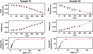
Standard image High-resolution imageFigure 7 shows the temperature dependence of peak position, line-width (FWHM) and the integrated intensity of observed excitonic peak in S1 and S2. Both these samples follow the Varshni's relation [27] for temperature dependence of their peak position. The temperature dependence of FWHM (ΓT) of PL spectra have been fitted to

where Γ0 is temperature independent contribution, Γ1 gives the measure of acoustic phonon contribution and the term having Γ2 contains the contribution from the longitudinal optical phonon [24, 28]. The LO-phonon energy hνLO is kept fixed at 72 meV as reported by Teke et al [29]. In both these samples Γ1 (0.23 meV K−1 for S1 and 0.29 meV K−1 for S2) ≪ Γ2 (0.33 eV for S1 and 0.43 eV for S2), hence the second term dominates at low temperatures, whereas at higher temperatures the third term predominates. Temperature dependence of the peak intensity is fitted to

where I01 and I02 are constants not depending on temperature and Ea is the activation energy of thermal quenching [24, 30]. The best fitted values obtained for Ea here are 19.4 meV for S1 and 16.5 meV for S2 implying that the carriers overcome the localized potential above ∼ 233 K for S1 and ∼ 198 K for S2 nano-structures. These observed differences in the fitted parameters for S1 and S2 clearly established the effect of morphological parameters on optical response of the nanostructures.
Figure 7. Temperature dependence of the excitonic peak position (□), FWHM (○) and integrated intensity (Δ) in samples S1 and S2. The dotted lines show respective theoretical model fit (discussed in text) to experimental points.
Download figure:
Standard image High-resolution image
4. Conclusions
We have reported the effect of the substrate temperatures on synthesis of ZnO nanostructures on Si substrates. Higher synthesis temperature favors the formation of the hexagonal and tapered nanorods, whereas the lower temperature leads to formation of nanoribbon-like structures. Formation of defect-free nanostructures at lower temperatures is reported. Further, geometrical effects in combination with the interfacial effects are reported to play an important role in the optical response of the nanostructures. Our observations show the strong dependence of stoichiometry, morphology and the optical properties on synthesis temperature and the interfacial properties of ZnO.