

Abstract
Graphene films were successfully synthesized by atmospheric pressure chemical vapor deposition (APCVD) method. Methane (CH4) gas and copper (Cu) tapes were used as a carbon source and a catalyst, respectively. The CVD temperature and time were in the range of 800–1000 °C and 10 s to 45 min, respectively. The role of the CVD temperature and time on the growth of graphene films was investigated in detail via scanning electron microscopy (SEM) and Raman spectroscopy techniques. The results of SEM images and Raman spectra show that the quality of the graphene films was improved with increasing of CVD temperature due to the increase of catalytic activity.
Export citation and abstract BibTeX RIS

Content from this work may be used under the terms of the Creative Commons Attribution 3.0 licence. Any further distribution of this work must maintain attribution to the author(s) and the title of the work, journal citation and DOI.
1. Introduction
Graphene is a two-dimensional material composed of carbon atoms arranged in a hexagonal atomic structure. Its theoretical thickness is about 0.34 nm [1, 2]. However, graphene has a number of properties which make it interesting for several different applications. It is the thinnest, mechanically very strong, transparent and flexible conductor [3]. The electron mobility of graphene is very high at room temperature (15000 cm2 V−1 s−1) which makes this material very interesting for electronic high- frequency applications such as high-frequency transistor and modulator [4]. Since graphene is the transparent electrode, it may be widely used in liquid crystal display (LCD), organic light-emitting display (OLED), where it can replace the rather fragile and expensive indium–tin–oxide (ITO) [5]. Established on large specific surface area, graphene is also used in gas detectors and biosensors [6, 7]. Besides, new types of composite material based on graphene with great strength and low weight could also become interesting for use in satellites and aircraft [8].
Most of these promising applications require the growth of graphene films in large areas on a suitable substrate. Graphene can be prepared by many methods. The first method is micromechanical cleavage from graphite. This method can only produce very small graphene films [9]. Recently, graphene has been produced by exfoliation and dispersion of graphite in organic solvents but the yield is very low [10]. The chemical exfoliation is an effective method to produce graphene film in large quantities [11]. However, chemical exfoliation involves complex chemical processes using heavily functionalized organic groups. Another way is epitaxial growth of graphene on silicon carbide (SiC) [12]. However, graphene grown on SiC substrates is difficult to transfer to other substrates. At present, thermal chemical vapor deposition (CVD) is one of the major methods to fabricate graphene [13]. With this method, the area and shape of graphene films are variable. In the thermal CVD process, at high temperature, hydrocarbon gases are decomposed, which leads to the formation of carbon atoms on the metal surface. These carbon atoms segregate and form graphene film.
In this work we report on APCVD method to grow large-area graphene films on copper (Cu) tape. There are a few reasons for the selection of Cu metal as a substrate: (i) carbon has a low solubility in Cu substrate, (ii) absence of a copper carbide and (iii) chemical etchant selectivity to graphene. Several parameters of APCVD such as time and temperature, which play important roles in graphene formation, were studied.
2. Experiment method
The graphene films were synthesized by thermal CVD method under high temperature (850–1000 °C) in argon (Ar) environment (1000 sccm). The Cu tapes with a thickness of 35 μm and a size of 0.5 cm × 0.5 cm were used as substrates for graphene-films synthesis process. To reduce the native copper oxide and to facilitate Cu grain growth on the Cu tape surface, the samples were annealed at CVD temperature for 30 min in a flow of Ar and hydrogen (H2, 300 sccm). After 30 min, a flow of methane (CH4, 30 sccm) was introduced for growth process (figure 1). The time for the CVD process ranged from 10 s to 45 min. After a preset graphene growth time, the samples were cooled rapidly under a flow of Ar (1000 sccm). The grown graphene films were then characterized using SEM, Raman spectroscopy and atomic force microscopy (AFM) techniques.

Figure 1. Plot of growth parameters for synthesis of graphene on Cu substrate.
Download figure:
Standard image High-resolution image3. Results of synthesis of graphene
3.1. Effect of growth temperature
One of the critical factors in synthesis of graphene is growth temperature because high energy is necessary to dissociate methane so that it reacts with the catalyst. To study the influence of the growth temperature on the synthesis of graphene, we executed the CVD process at different temperatures 850, 900, 950 and 1000 °C for the same time and gas flow (30 min and Ar/H2/CH4 = 1000/300/30 sccm flow rates). The shape and the size of graphene patches referred to as domains can be imaged by SEM. Figure 2 is the SEM images which shows the effect of growth temperature on the formation of the graphene while keeping time and gas flow rates unchanged. Figure 2 shows that the density and size of graphene domains increase with increasing temperature. The graphene grown at 850 °C has domains of about 100–200 nm size. Meanwhile, the graphene grown at 900 °C produces domains of about 1–3 μm size. At higher temperature the domains spread and at growth temperatures of 950 and 1000 °C (figures 2(c) and (d)) graphene films covered the whole surface of the Cu tape. Borders of the graphene films appear clearly on the surface of the Cu tape. These results are due to the increase of the precursor activity at high temperature.
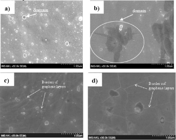
Figure 2. SEM images of the Cu tape's surface after CVD process for 30 min at different temperatures: (a) 850 °C, (b) 900 °C, (c) 950 °C, and (d) 1000 °C.
Download figure:
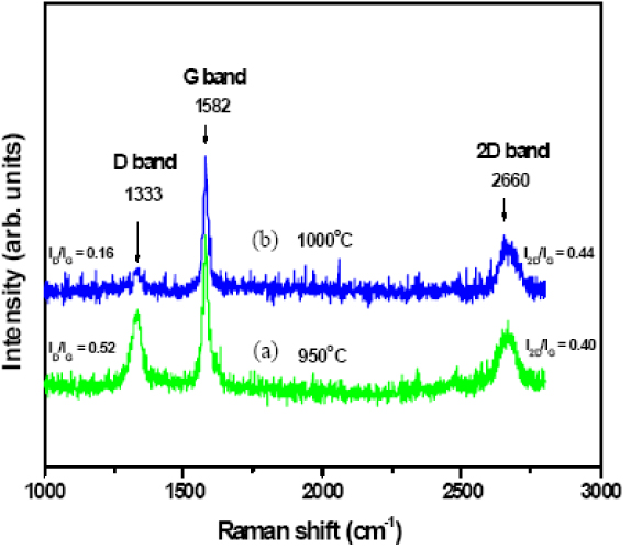
Standard image High-resolution imageIt is known that Raman spectroscopy is a powerful, yet relatively simple method to characterize the thickness and crystalline quality of graphene layers [14, 15]. Raman spectroscopy was performed under excitation laser (λ = 632.8 nm) on the CVD grown graphene. Figure 3 shows Raman spectra of the graphene film grown on the Cu substrate surface at CVD temperatures of 950 and 1000 °C. Raman spectra of two samples grown at 950 and 1000 °C show three Raman peaks at 1333 cm−1 (D band), at 1582 cm−1 (G band) and at 2660 cm−1 (2D band). The D band indicates the defective and impure structure of graphite sheets. The G band indicates the order and purity structure of graphite sheets. The 2D band is the characteristic peak of graphene structure. It is known that the ratio I2D/IG of the intensity I2D and IG of the bands 2D and G is dependent on the number of graphene layers [14, 15]. The ratio I2D/IG ∼ 2–3 is for monolayer graphene, 2 > I2D/IG > 1 for bilayer graphene and I2D/IG < 1 for multilayer one. Based on the ratio I2D/IG of Raman spectra, it can be concluded that the graphene films grown on the Cu tape at 950 and 1000 °C are multilayers. The graphene films grown at 1000 °C have higher ratio I2D/IG and lower ratio ID/IG compared to those of the graphene films grown at 950 °C. These results show that the CVD temperature of 1000 °C is the optimum temperature for growing high-quality graphene films on the Cu tape surface.

Figure 3. Raman spectra of the graphene film grown on the surface of the Cu substrate at different temperatures: (a) 950 °C and (b) 1000 °C.
Download figure:
Standard image High-resolution image3.2. Effect of growth time
Figure 4 shows SEM images of graphene films grown on Cu tape surface with the growth time ranging from 10 s to 45 min at 1000 °C under flow of CH4 and H2 (CH4/H2 = 30/300 sccm). The dark features in the SEM images in figures 4(a)–(c) correspond to the graphene domains and the bright regions are the bare Cu. It is clear that the graphene domains grown during 10 s are smaller than that grown during 30 s (figures 4(a) and (b)). The formed graphene area increases with the growth time increasing. Figure 4(d) indicates that after 5 min of growing, the entire surface of the copper foil is covered with graphene. This shows that the carbon atoms actively move in and out of the edges of the graphene sheet till all the growth domains are linked, forming a solid and stable graphene sheet.

Figure 4. SEM images of graphene films grown on the Cu tape's surface after CVD process for (a) 10 s, (b) 30 s, (c) 1 min, (d) 5 min, (e) 30 min and (f) 45 min.
Download figure:
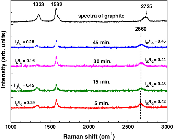
Standard image High-resolution imageFigure 5 shows a comparison of the Raman spectra of the graphite and the graphene films grown on the surface of the Cu with the growth time ranging from 5 min to 45 min. The Raman spectra show that the 2D band of the graphene films shifts to short wavelength (2660 cm−1) compared to wavelength (2725 cm−1) of the bulk graphite. The ratio of I2D/IG does not change much. This value changes from 0.42 (for 5 min of growing) to 0.45 (for 45 min of growing). But the ratio of ID/IG changes clearly. For growing time of 30 min, the ratio ID/IG is lowest (with the value of 0.16). It indicates that the quality of the graphene is the best. These results show that the number of layers of graphene seemingly do not change clearly over growth time and the growth time of 30 min is optimum.

Figure 5. Comparison of the Raman spectra of the graphene films grown on the surface of the Cu and graphite measured at 632.8 nm.
Download figure:
Standard image High-resolution imageAlthough the growth time does not affect much the number of layers of graphene, the number of layers of graphene depends on the morphology of the Cu substrate. At a constant temperature, the CH4 decomposition rate on an ideal flat Cu surface should be uniform. However, the Cu tape used for graphene growth is not single crystal, there are many atomic steps and grain boundaries even after annealing. These sites usually have much higher chemical activation energy than those of the flat regions of Cu. Therefore, hydrocarbons prefer to decompose on the sites with high activation energies (such as grain boundaries and surface steps) to form nucleation centers. Detailed description on the effect of Cu surface to the growth of high-quality graphene was also published in [16].
Figure 6(a) shows the SEM image of the graphene domains on the surface of the Cu tape after CVD process at 1000 °C for 30 min. There are two different visibly contrasting regions in the SEM image. The regions with A circle and with B circles are few-layer and multilayer structures, respectively. Figure 6(b) shows the Raman spectra measured on two different points of graphene film. The ratio of I2D/IG is 0.84 and 0.44 for the few-layer and multilayer graphene film, respectively. The 2D band of the few-layers graphene shifts to short wavelength (at 2650 cm−1) compared to wavelength (at 2660 cm−1) of the multilayer graphene.
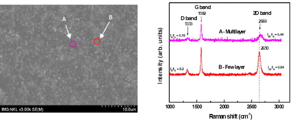
Figure 6. SEM image (a) and Raman spectra (b) of the graphene domains on the surface of the Cu tape after CVD process at 1000 °C for 30 min.
Download figure:
Standard image High-resolution imageTo estimate clearly the thickness of the graphene film, we transferred the graphene film from the Cu tape to glass substrate (figure 7(a)) and measured the difference between the height of the graphene film and the glass substrate using AFM. Figure 7(b) shows the AFM image of the graphene film after transferring from the Cu tape to silicon substrate. AFM image indicates that the thickness of the graphene film was about 5 nm; this means that the grown graphene films are multilayer (about 15 layers). The thickness of the graphene is only 5 nm, so the transmission of the graphene film is very high. We can see clearly the word of IMS-VAST covered by the graphene film (figure 7(a)).

Figure 7. (a) Photo and (b) AFM image of the graphene film after transferring from the Cu tape to the glass substrate.
Download figure:
Standard image High-resolution image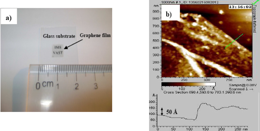
4. Conclusion
Multilayer graphene films were successfully synthesized on the Cu tapes by APCVD method. The quality of the graphene films was improved with increasing CVD temperature. The growth time does not much affect the number of layers of graphene films. CVD temperature of 1000 °C and CVD time of 30 min are the optimum temperature and time for growing high-quality graphene films on the Cu tape, respectively. The graphene films were successfully transferred from the Cu tape to other substrates by wet etching Cu with a solution of iron(III) nitrate. This opens a promising way for application of graphene films in LCD, OLED electronic devices, in gas detectors and biosensors.
Acknowledgments
The authors acknowledge financial support from projects of the Key Laboratory for Electronic Materials and Devices, IMS (grant HTTD 01.12), Vietnam National Foundation for Science and Technology Development (NAFOSTED, code 103.99–2012.15). Besides, this work is supported from projects of Director of IMS and Young scientist of VAST 2012.