

Abstract
Micro-electro-mechanical systems (MEMS) sensors have movable parts: thus, it is difficult to handle them at fabrication because of the possibility of fracture. If a MEMS sensor could be fabricated not only on a silicon substrate but also on a ceramic substrate, which can be used for a package of the end product, the above-mentioned problem about handling would be solved, and its fabrication cost would be reduced. In this presentation, as demonstrations of the sensors directly fabricated on a ceramic package, an accelerometer and a magnetoresistive (MR) sensor are focused on. A micro accelerometer is proposed, which consists of a proof mass and ferroelectric substrate under it. A screen-printed barium titanate (BTO) film on an alumina substrate was employed as ferroelectrics. The sensitivity of the fabricated accelerometer was 0.1 pF g−1. A triaxis MR sensor is proposed, which detects not only x- and y-axes' magnetic field intensities but also that of the z-axis. Namely, not only azimuth but also angle of elevation of the sensor can be detected from triaxis components of the geomagnetic field. A permalloy (FeNi) plate is stood aside from the MR element. The plate distorts magnetic field and generates the x- (or y-) component from the originally z-directional field. A triaxis geomagnetic field was successfully detected by the fabricated sensor.
Export citation and abstract BibTeX RIS

Content from this work may be used under the terms of the Creative Commons Attribution-NonCommercial-ShareAlike 3.0 licence. Any further distribution of this work must maintain attribution to the author(s) and the title of the work, journal citation and DOI.
1. Introduction
Micro-electro-mechanical systems (MEMS) sensors generally have movable parts; thus, it is difficult to handle those sensors at fabrication because of the possibility of fracture. There is a report claiming that assembling cost and testing cost occupy 80% of the unit price of a MEMS sensor (www.memunity.org/on wafer_testing.htm). If a MEMS sensor could be fabricated not only on a conventional silicon-based substrate but also on a ceramic substrate, which can be used for a package of the end product, the above-mentioned problem about the handling of MEMS sensors would be solved, and its fabrication cost would be reduced drastically. The schematic illustration of the MEMS sensors on a ceramic package is shown in figure 1.
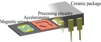
Figure 1 Concept of a MEMS sensor directory fabricated on ceramic package. In this system, signal processing circuits for the sensors are also integrated.
In the present paper, as demonstrations of the sensors directly fabricated on a ceramic package, an accelerometer and a magnetoresistive (MR) sensor are focused on, and their fabrication on a ceramic substrate is investigated.
2. Accelerometer using screen-printed (BTO) film
We have already proposed a new type accelerometer, which uses a ferroelectric material and its fringe capacitance, as shown in figure 2 [1]. There is an interdigitized pair of comb-shaped anode and cathode electrodes under an insulating proof mass, and the fringe electrical field between the two electrodes is used in order to detect the acceleration input to this sensor. Therefore, this sensor can be fabricated easily because surface micromachining is applicable. When the proof mass moves vertically by the acceleration, a volume ratio of the ferroelectrics and air, which are penetrated by the line of electric force, is changed. And then, the relative dielectric constant ε r between the opposed pair of electrodes is equivalently changed. Namely, this sensor uses change in the ε r in capacitance C, which is given by the following equation:

where ε 0 is the dielectric constant of the air, S is the overlapping area of two electrodes, and d is the distance between the two electrodes. Therefore, it is important to use highly dielectric material for this sensor.
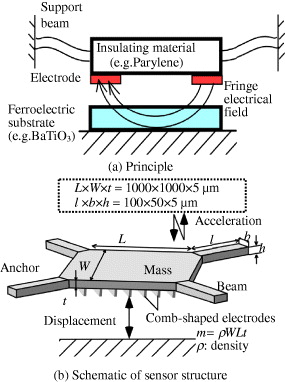
Figure 2 Accelerometer using ferroelectrics.
In our previous study on the accelerometer, the capacitors are fabricated on a bulk ferroelectric plate of lead zirconium titanate (PZT) (Pb(Zr,Ti)O 3, ε r is approximately 2600) for enhancing the sensitivity of accelerometer (figure 2) [1]. However, the fabrication cost was high because the PZT plate is expensive. In the present paper, we succeed in preventing the fabricating cost of the accelerometer using a screen-printed film of BTO (BaTiO 3, ε r is 900–1000) on an alumina substrate, instead of using a PZT bulk plate. The screen-printing method can save the amount of raw material of the film, because a comparatively thick film can be deposited only on a specified area. In this study, BTO pastes are transferred on an alumina substrate through aperture holes of the screen. Additionally, the BTO is safer for human bodies than the PZT, because the BTO does not contain harmful lead, unlike PZT. A platinum (Pt) film is screen-printed under the BTO film, since Pt serves as a barrier metal layer for blocking the oxygen outgas from the glaze layer of the alumina substrate during the annealing [2]. The BTO paste was fabricated by hydrothermally synthesizing BTO powder with ethylcellulose and terpineol, followed by screen-printing it on an alumina substrate. Then, the film was annealed at 1400 °C by a rapid-heating oven. The fabrication condition is shown in table 1. The scanning electron microscopy (SEM) image of the resultant BTO film is shown in figure 3, proving that the BTO film is crystallized.
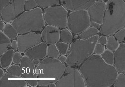
Figure 3 SEM image of BaTiO 3 film on Pt.
Table 1. Annealing conditions of Pt and BaTiO 3 film.
| Pt | 2 | 120 °C | 1400 °C | N/A |
| BaTiO 3 | 2 | 150 °C | 1400 °C | 14–17 |
We fabricated an accelerometer using the crystallized BTO film. The process flow of is shown in figure 4. An experimental setup for characterizing the fabricated accelerometer is shown in figure 5. The capacitance of the accelerometer is translated to the voltage by a capacitance–voltage (CV) conversion IC (MB42M001, Fujitsu Limited). The output of the accelerometer was measured by an electric tester. Here, positive gravitational acceleration (+g) is applied to the accelerometer when the fixture is at normal position. On the other hand, negative gravitational acceleration (−g) is applied when the fixture is turned over.
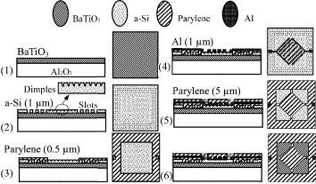
Figure 4 Process flow of accelerometer.
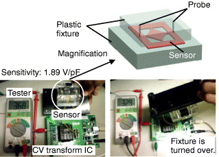
Figure 5 Measurement system for ±g acceleration (g: gravitational acceleration).
Measurement results are shown in table 2. The sensitivity of the fabricated accelerometer was 0.1 pF g−1, the order of which is the same as that of the previously developed accelerometer using a PZT substrate (0.4 pF g−1) [1].
Table 2. Results of capacitance change.
| Sensor+wiring | ||
| + 1 g | 2.94 | 0.20 |
| −1 g | 2.74 | |
| Wiring only | ||
| + 1 g | 1.71 | 0.06 |
| −1 g | 1.65 |
3. Triaxis MR sensor using permalloy plate of distorting magnetic field
Recently, a navigation system of directing a user to an objective point has been installed in mobile devices such as cell phones, personal digital assistant (PDA) devices and so on. A magnetic azimuth sensor is usable for detecting the orientation of the user: therefore, miniaturizing a magnetic sensor to the extent that it could be installed in a mobile device is desired. Magnetic azimuth sensors have been reported based on MR method, which detects MR resistance change due to magnetic field change [3]. An azimuth sensor composed of MR elements and a planer coil, which can be fabricated by surface micromachining technique, was reported [4]. Our study basically refers to this sensor and adds a triaxis function to it.
Permalloy (FeNi) resistor changes its resistance with respect to applied magnetic field, as shown in figure 6. To convert resistance change to voltage, the Wheatstone bridge is employed for one axis measurement, as shown in figure 7 (note that two bridges for x- and y-direction are included in this figure). To obtain a large rate of resistance change ΔR/R, bias magnetic field is applied using a planar coil, as shown in figure 8(a). Then, the inclination of ΔR/R per applied magnetic field change becomes steeper. Note that the bias direction for R1, R3 and that for R2, R4 are opposite, so R1, R3 decrease and R2, R4 increase, as the applied field increases, as shown in figure 8(b). Output voltage is expressed as (ΔR/R)E, where E is the source voltage.
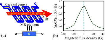
Figure 6 Permalloy resistance R changes with respect to magnetic field H =μ0 B , where μ0 is permeability of air, B is flux density, (a) in case the angle between electric current and magnetic field is rectangular, (b) ΔR/R changes experimentally with respect to the intensity of B .
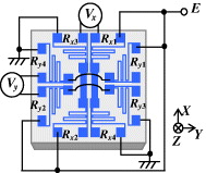
Figure 7 Schematic sensor composition. It comprises two Wheatstone bridges for detecting x- and y-axes' magnetic field intensities.
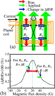
Figure 8 Principle of detecting applied magnetic field along one axis, (a) bias magnetic field is applied using a planar coil, (b) then, the inclination of ΔR/R per applied magnetic field becomes steeper. Note that R1, R3 decrease and R2, R4 increase, as the applied field increases.
The sensor shown in figure 7 can detect magnetic azimuth because it has two bridges for detecting magnetic fields along x- and y-axes. However, it is impossible to detect both horizontal azimuth and angle of elevation at the same time. To detect also the angle of elevation, one more sensor should be set orthogonally to the azimuth sensor, as shown in figure 9(a). The total sensor height is, however, increased, causing the packaging problem in mobile electronic devices. Therefore, a sensor which can detect all the three axes fields with reasonable thinness is proposed in this study, as shown in figure 9(b). In this figure, a permalloy (FeNi) plate is stood aside from the MR element. Here, magnetic field around the plate is once converged inside the plate and then released outward, generating the x-directional field on the sensor surface from the originally z-directional magnetic field, as shown in the enlarged cross section in figure 9(b).
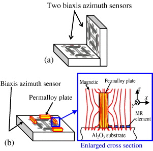
Figure 9 Advantage of space efficiency, (a) conventional method of using two orthogonal azimuth sensors, (b) proposed sensor for detecting all axes components of the magnetic field.
The fabrication process of the proposed sensor is shown in figure 10. Here, MR elements made of permalloy are annealed to improve their MR property. Annealing gas of H 2 and annealing temperature of 400 °C are searched and defined by preliminary experiments. Figure 11 shows a photograph of the MR sensor before and after fabricating the planer coil. Permalloy plates of distorting magnetic field were bonded by adhesive resin.
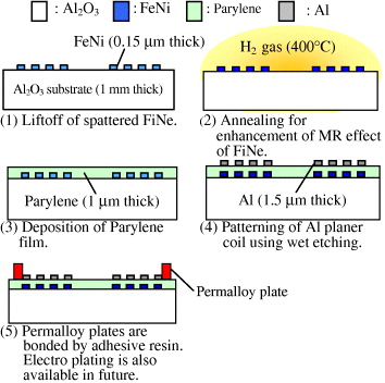
Figure 10 Fabrication process of triaxis MR sensor device.
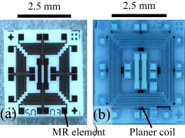
Figure 11 Photograph of fabricated MR sensor (a) before, and (b) after fabricating the planar coil.
The fabricated sensor is set on a rotational table, as shown in figure 12. In this preliminary experiment, only one permalloy plate was set adjoining Rx1, and the sensor was rotated around only one axis. The output voltage of the Wheatstone bridge was measured by changing the rotational angle around each axis of the sensor every 30° in the geomagnetic field. The results are shown in figure 13. By using a permalloy plate, the normalized bridge output sinusoidally changes with respect to the rotational angle around the x-axis. The amplitude of change is larger compared to that without the plate. The fabricated sensor using a permalloy plate is proved to clearly detect the triaxis magnetic field, even it is a subtle geomagnetic one.
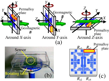
Figure 12 (a) Experimental setup for geomagnetic field measurement. Bridge output Vx was estimated by changing rotational angle around each axis of the sensor, (b) photograph of sensor rotated around its z-axis, and (c) position of permalloy plate.
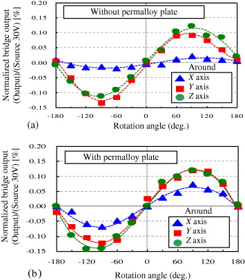
Figure 13 Relationship between normalized bridge output and rotational angle in geomagnetic field around each axis of the sensor, (a) without, (b) with permalloy plate. The amplitude around the x-axis of the latter is approximately 7.5 times larger than that of the former.
4. Conclusion
The concept of MEMS sensors directly fabricated on a ceramic substrate, which can be used for a package of the end product, was proposed. An accelerometer using a BTO film and a triaxis MR sensor for detecting not only x- and y-axes' magnetic field intensities but also that of the z-axis were practically fabricated on a ceramic alumina substrate.
Acknowledgments
This work was supported in part by JSPS (Japan Society for the Promotion of Science) KAKENHI (22310083). This work was supported in part by the Kansai University Special Research Fund, 2010: 'Development of a MEMS Multi-Sensor for Mobile Devices'.