
Abstract
One of the main requirements for ultra-large-scale integrations (ULSIs) is atomic-order control of process technology. Our concept of atomically controlled processing is based on atomic-order surface reaction control by CVD. By ultraclean low-pressure CVD using SiH4 and GeH4 gases, high-quality low-temperature epitaxial growth of Si1−xGex (100) (x=0–1) with atomically flat surfaces and interfaces on Si(100) is achieved. Self-limiting formation of 1–3 atomic layers of group IV or related atoms in the thermal adsorption and reaction of hydride gases on Si1-xGex (100) are generalized based on the Langmuir-type model. By the Si epitaxial growth on top of the material already-formed on Si(100), N, B and C atoms are confined within about a 1 nm thick layer. In Si cap layer growth on the P atomic layer formed on Si1−xGex (100), segregation of P atoms is suppressed by using Si2H6 instead of SiH4 at a low temperature of 450 °C. Heavy C atomic-layer doping suppresses strain relaxation as well as intermixing between Si and Ge at the Si1−xGex/Si heterointerface. It is confirmed that higher carrier concentration and higher carrier mobility are achieved by atomic-layer doping. These results open the way to atomically controlled technology for ULSIs.
Export citation and abstract BibTeX RIS

Content from this work may be used under the terms of the Creative Commons Attribution-NonCommercial-ShareAlike 3.0 licence. Any further distribution of this work must maintain attribution to the author(s) and the title of the work, journal citation and DOI.
1. Introduction
Atomically controlled processing for group IV semiconductors has become indispensable for ultra-large-scale integrations (ULSIs), because high performance devices require atomic-order abrupt heterointerfaces and doping profiles as well as strain engineering due to introduction of Ge and C into Si. Especially for processing involving surface reaction processes like chemical vapor deposition (CVD), the advancement requires atomic-order surface reaction control. Improvements in the quality of gases and equipment have enabled ultraclean low-temperature CVD processing for atomic-order control [1–3].
Our concept of atomically controlled processing is based on atomic-order surface reaction control by CVD [3–5]. The final goal is the generalization of the atomic-order surface reaction processes and the creation of new properties in Si-based ultimate small structures which will lead to nanometer scale Si devices (figure 1). Based on the investigation of surface reaction processes, the concept has been demonstrated for high performance Si 0.65 Ge 0.35 channel p-type metal-oxide semiconductor field-effect transistors (pMOSFETs) with a 0.12 μm gate length by utilizing in situ impurity-doped Si 1−x Ge x selective epitaxy on the source/drain regions at 550 °C [6]. In in situ doped Si 1−x Ge x epitaxial growth on the (100) surface in a SiH 4–GeH 4-dopant (PH 3 or B 2 H 6 or SiH 3 CH 3)–H 2 gas mixture, the growth characteristics have been expressed quantitatively by modified Langmuir-type rate equations [3, 5].
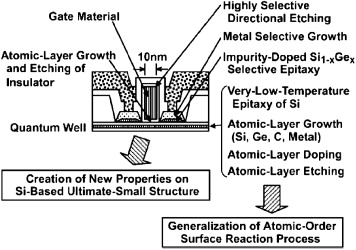
Figure 1 Atomically controlled processing of group IV semiconductors for ULSIs.
In this paper, the self-limited surface reactions of hydride gases on Si 1−x Ge x (100) (x=0−1) for atomic-order growth are reviewed based on the Langmuir-type adsorption and reaction scheme. Furthermore, typical atomic layer (AL) doping by the epitaxial growth of Si on top of doped material formed on (100) surface and their capability of atomically controlled processing for ULSIs are discussed.
2. Atomic-order reaction of hydride gas on Si 1−x Ge x surface
Hydrogen terminating on the Si 1−x Ge x (100) surface desorbs by heating the substrate. This hydrogen desorption initiates adsorption and reaction of reactant gas. Self-limiting characteristics [3, 5, 7] are observed in many cases (table 1) and are explained based on kinetics of Langmuir-type adsorption models (figure 2) [3, 5].
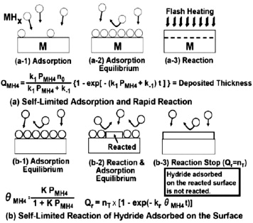
Figure 2 Schematic images of (a) self-limited adsorption and (b) self-limited reaction of hydride for atomic-order growth based on Langmuir-type model.
Table 1. Typical self-limiting conditions for some hydride gases on Si 1−x Ge x (100) surface.
| SiH 4/Si | 385 | 100−500 | Flash. Ad.–Desorp. Equil. |
| SiH 4/Ge | 260 | 10−500 | Thermal, 1AL |
| GeH 4/Ge | 268 | 2.9−13 | Flash, 1AL |
| CH 4/Si | 500−600 | 50−1600 | Thermal, 2ALs |
| NH 3/Si | 400 (300−800) | 124−1400 | Thermal and flash, 2, 4ALs |
| NH 3/Si 0.5 Ge 0.5 | 400 | 550 | Thermal, 3ALs |
| NH 3/Ge | 400 | 550 | Thermal, 1AL |
| PH 3/Si | 450 | 0.26 | Thermal, 3ALs |
| PH 3/Ge | 300 | 0.26 | Thermal, 1AL |
| B 2 H 6/Si | 180 | 1−3×10⁻³ | Thermal, 2ALs |
| SiH 3 CH 3/Si | 450 | 18 | Thermal, 1AL |
| SiH 3 CH 3/Ge | 450 | 18 | Thermal, 1AL |
In the case of SiH 4 and GeH 4 adsorption on monohydride Si(100) and Ge(100) surfaces, respectively, the adsorption proceeds according to Langmuir-type kinetics shown in figure 2(a). The adsorbed SiH 4 and GeH 4 do not react and desorb by removing SiH 4 and GeH 4 gases in the reactor. In order to perform atomic-layer growth, the reaction must be induced during the short interval by the method such as flash heating, in which the next adsorption scarcely proceeds.
In the other cases, NH 3 on Si, SiH 4 on Ge (100), CH 4 on Si(100) and SiH 3 CH 3 on Si(100) and Ge(100) are also described by the equation in figure 2(b). Especially, in the case of the SiH 4 reaction, it was found that one-atomic-layer growth of Si occurs on the hydrogen-free surface formed by preheating at 350 °C in Ar, and sub-atomic-layer growth on the hydrogen-terminated surface with the dimer structure formed by preheating at 350 °C in H 2. The density of the SiH 4 reaction sites on the hydrogen-terminated Ge surface with the dimer structure is lower than that on the hydrogen-free surface. In the case of PH 3 reaction, the P atomic amount on the surface tends to saturate below one atomic layer on the Ge(100) surface at 300−450 °C, and two or three atomic layers on the Si(100) surface at 450−750 °C. In the case of B 2 H 6, the B atom amount tends to saturate self-limitedly at around 1.4×1015 cm −2 (2 ALs) at 180 °C (Figure 3) [7]. At 500 °C, the B atomic amount increases with B 2 H 6 exposure time and exceeds 2 ALs. It is clear that continuous B 2 H 6 reaction at 500 °C proceeds with H desorption on B atoms.
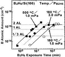
Figure 3 B 2 H 6 exposure time dependence of B atom amount on Si(100) at 180 and 500 °C.
These results mean that the reaction site density depends on not only substrate surface structure but also hydride gas species and substrate temperature.
3. Atomic layer doping in Si 1−x Ge x epitaxial growth
On the nitrided Si(100) surface formed by NH 3 reaction at 400 °C, the Si film is epitaxially grown by SiH 4 exposure at 500 °C with an incubation period, while the deposition rate after the incubation period is the same as that on the Si surface. After Si cap layer growth, most of the N atoms are buried in the initially nitrided region within the thickness of about 1 nm, that is within the measurement accuracy. For multi-layer N-doped Si film composed of N layers of 1×1014 cm −2 and 3 nm thick Si spacer, N atoms act as a donor. The sheet carrier concentration is about 5×1011 cm −2 per layer. The Hall mobility is much larger than that (about 100 cm 2 (V·s)−1 at 300 K) of the uniformly P-doped Si with P concentration of 1019 cm −3, and is as high as that of 1016−1017 cm −3 [10]. Because the local concentration of the ionized donor is estimated to be about 1018−1019 cm −3 in 1 nm thick N-doped region, it is considered that scattering in electron transport is reduced by atomic layer doping structure and that the carrier mobility is enhanced by highly condensed strain near the N atomic layer-doped region [5].
On the P layer formed on the Si(100) surface, Si epitaxial growth is achieved at a rather high SiH 4 partial pressure of 220 Pa at a rather low temperature of 450 °C [5]. Although the P desorption from the Si surface and the P incorporation into the over-layer Si films are found, a Si/4×1014 cm −2 P/Si epitaxial film is prepared and it shows very high carrier concentration and very low resistivity compared with doping under thermal equilibrium conditions. Using such atomic-layer doping of P, very low contact resistivity between Ti and the Si film is obtained to be about 5×10⁻⁸ Ωcm 2 [5]. In unstrained Si cap layer growth on the P atomic layer formed on Si 1−x Ge x (100) with the P atomic amount below about 4×1014 cm −2 using Si 2 H 6 instead of SiH 4 [8], the incorporated P atoms are almost confined within 1 nm around the heterointerface [9]. It is found that tensile-strain in the Si cap layer growth enhances P surface segregation and reduces the incorporated P amount around the heterointerface (figure 4) [9]. The electrical inactive P atoms are generated by tensile-strain in heavy P-doped region [10].
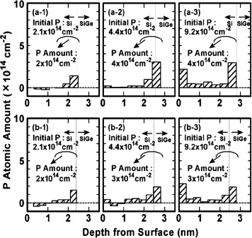
Figure 4 Depth profiles of P for Si/P/Si 0.3 Ge 0.7 on (a) unstrained Si(100) (upper) and (b) 0.8% tensile-strained SOI (lower). Initial P atomic amount was about (a-1)(b-1) 2.1×10¹⁴, (a-2)(b-2) 4.4×10¹⁴ and (a-3)(b-3) 9.2×1014 cm −2. Si cap layer was deposited at 450 °C at Si 2 H 6 partial pressure of 20 Pa. Interface depths were estimated from decay characteristics of Ge 3 d XPS intensity. Because the P amount was calculated by combination of XPS measurement and wet chemical etching of subnanometer-thick Si layer, there are negative values due to experimental error.
By Si epitaxial growth with SiH 4 reaction at about 7×1014 cm −2 B atomic layer formed with B 2 H 6 reaction at 180 °C on Si(100) surface, most of the incorporated B atoms are confined within an about 1 nm thick region [11]. However, the sheet carrier concentration is as low as 1.7×1013 cm −2. The electrical inactive B could be a result of clustering of surface B atoms just before Si growth at 500 °C. Additionally, by heavy B-doping, strain could be induced. For in situ B-doped Si epitaxial growth on 0.8%-tensile-strained Si(100)-on-insulator (SOI) at 550 °C, the B concentration region in which carrier concentration is almost equal to the B concentration is lower, compared with that on the unstrained SOI (figure 5 ) [12]. It is suggested that, for in situ B-doped Si epitaxial growth, the substitutional B and the interstitial B concentrations in the unstrained Si are higher and lower than those on tensile-strained Si, respectively.
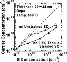
Figure 5 Carrier concentration versus concentration in in situ B-doped Si.
It was confirmed that the intermixing at the Si/Si 1−x Ge x /Si heterointerface is suppressed by carbon atomic-layer doping at the heterointerface for the heat-treatment for 3 h at 650 °C [13]. In the case of 40 nm thick strained Si 0.55 Ge 0.45/Si, the strain amount is reduced by the carbon atomic-layer doping of (1–3)×1014 cm −2 at the heterointerface and the reduction becomes larger with the heat treatment. While, in the case of 4 nm thick strained Si 0.55 Ge 0.45/Si, strain relaxation as well as intermixing between Si and Ge are suppressed, although Ge fraction for the undoped heterostructure is reduced and the strain comes to be relaxed after the 650 °C heat treatment (figure 6).
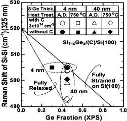
Figure 6 Ge fraction dependence of Raman shift of Si-Si peak in 4 and 40 nm thick Si 1−x Ge x cap layer/Si(100) heterostructures with and without C atomic layer doping before and after heat treatment at 750 °C for 3 h. Initial Ge fraction is about 0.45. Solid and dashed lines are the values for fully strained and relaxed Si 1−x Ge x films, respectively.
4. Conclusion
Self-limiting formation of 1–3 atomic layers of group IV or related atoms in the thermal adsorption and reaction of hydride gases on Si 1−x Ge x (100) surface are generalized based on the Langmuir type model.
Atomic layer doping results of N, P, B and C indicate that very high carrier concentration and higher carrier mobility of Si-based group IV semiconductors could be achieved compared with doping under equilibrium conditions, and that suppression of intermixing and strain relaxation at the heterointerface are obtained.
These results open the way to atomically controlled technology for channel engineering, heavy impurity doping in ULSIs.
Acknowledgments
The study was partially supported by a Grant-in-Aid for Scientific Research from the Ministry of Education, Culture, Sports, Science and Technology of Japan.