
Abstract
Polymethyl methacrylate (PMMA) has been proposed as a material for micro-electromechanical systems (MEMS) to initiate the research on environmentally friendly micro-nano machining technology using polymer materials. A polymer MEMS process has been developed using hot embossing and precision machining. MEMS structures less than 2 μm were successfully embossed. The PMMA layer that remained after hot embossing was removed by a polishing process to release the movable parts. A PMMA electrostatic comb-drive microactuator was fabricated. Both finger width and gap between fingers were 5 μm, and thickness was larger than 70 μm. An operated displacement of 11 μm at a drive voltage of 100 V was obtained. It was 20 times larger than that of an identical silicon device. A torsional micro mirror device driving with vertical comb actuator was fabricated. The size of the mirror was 1×1 mm2. The maximum tilt angle of 5.6 was obtained with driving voltage of 100 V and frequency up to 100 Hz. A chevron-shaped PMMA thermal actuator with a thickness of about 50 μm has been fabricated and tested successfully. The displacement was about 5 times larger than that of a Si counterpart at the same power consumption.
Export citation and abstract BibTeX RIS

Content from this work may be used under the terms of the Creative Commons Attribution-NonCommercial-ShareAlike 3.0 licence. Any further distribution of this work must maintain attribution to the author(s) and the title of the work, journal citation and DOI.
1. Introduction
Research on micro-electromechanical systems (MEMS) is a basic part of the leading edge technology for future development of the semiconductor IC industry. Within this development it is necessary to create the foundation of sustainable, environmentally friendly production systems. Nowadays, in semiconductor- and advanced technology-based industries, silicon and petroleum-based polymers are being used as key materials, but unfortunately these materials are not sustainable and not environmentally friendly. Considering the above facts, it is necessary to initiate research on MEMS with environmentally friendly micro-nano machining technology using bio-based polymer materials, and the industrialized technology of applied devices (microsensors, actuators, μ-TAS, etc). This research is part of the initiation of R&D on polymer MEMS. Polymer materials have several advantages over silicon material, such as much lower stiffness, transparency, higher coefficient of thermal expansion, better biocompatibility and the fact that they are environmentally friendly [1], lower material cost, and easier fabrication by mass-replication technologies, e.g. injection molding, hot embossing [2]. The transparency of PMMA is important for optical devices, such as lenses, waveguides, etc [3], and optical-based biomedical or microfluidic devices. Small Young's modulus and high thermal expansion of PMMA are the advantages for electrostatic and thermal actuators [4], respectively, because it will require less power than silicon counterparts to produce the same displacement.
Recently, photoresist-based vertical comb actuators were developed by using the UV-lithography method [5]. The fabrication process was simple, however, the polymers were limited to photoresist-based polymers, and the device was not monolithic since a glass substrate was used as a carrying wafer. In another work, lateral PMMA electrostatic comb actuator was fabricated by hot embossing and O 2 plasma etching [6]. However, heat generation during the O 2 plasma strongly affected the surface of the device. In our group, recently in [2], ultra-precision cutting was used to remove the thin PMMA layer remaining after the hot embossing process. However, ultra-precision machining has low productivity and high cost. In this study, we develop a high-efficiency and low-cost fabrication process for polymer MEMS devices with a wide range of material selectivity. For this purpose, hot embossing and polishing are the main processes to be used. This fabrication process will not require the high-cost semiconductor manufacturing equipment used for silicon micromachining. Consequently, the process is compatible with wafer-level and the equipment cost is substantially reduced. Basically, our proposed method can be applied for varieties of polymers, and the development of polymer-MEMS devices is straightforward.
In this paper, PMMA is used as structural material for MEMS actuators and sensors to utilize its advantage of small Young's modulus and high thermal expansion coefficient and good compatibility for the hot embossing process. An electrostatic comb-drive microactuator, a torsion mirror, a thermal actuator and a microaccelerometer were fabricated, demonstrated and evaluated.
2. Fabrication process
2.1. Hot embossing process flow for polymer MEMS
The fabrication process of the polymer MEMS is shown schematically in figure 1. First, a two-step Si mold was fabricated by deep reactive ion etching (RIE) (figure 1(a)), and then the device structures were formed by the hot embossing process (figure 1(b)). Then, the sample was bonded to another PMMA substrate by the surface activation method to create a firm bonding without using intermediate material (figure 1(c)). A PMMA layer with a thickness of more than 10 μm always remains after the hot embossing process. In order to release the movable structures, this layer was removed efficiently by using the polishing method (figure 1(e)). This method can process a large number of devices at the same time and provides a mirror-finished surface. The polishing process started with grit size of 1 μm and ended up with grit size of 0.05 μm. To protect the PMMA microstructures from fracture and deformation during the polishing process, reinforcement material was filled into the gaps of embossed PMMA structures (figure 1(d)). After the polishing process, reinforcement material was self-evaporated in vacuum, and the freestanding PMMA movable microstructures were successfully released. Finally, a gold layer was sputtered to the surfaces of the PMMA micro device to create the electrode for the actuators (figure 1(f)).
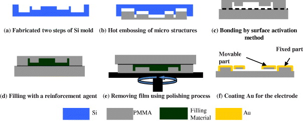
Figure 1 Fabrication process of PMMA movable micro devices.
2.2. Fabrication of two-step Si mold
The fabrication process of the two-step Si mold is shown schematically in figure 2 [7]. Firstly, SiO 2 layer was formed on the surface of a Si wafer by thermal oxidation process, and then movable parts and fixed parts were patterned by photolithography and SiO 2 etching by BHF acid (figure 2(a)). Next, the fixed parts were patterned by photolithography to create a photoresist mask for the inductively coupled plasma reactive ion etching (ICP-RIE) process (figure 2(b)). Then, the ICP-RIE process was performed to a depth of 56 μm (figure 2(c)). Next, photoresist was removed and the second ICP-RIE process was performed (with the etching mask SiO 2) to a depth of 84 μm, and the patterns of a movable part were created (figure 2(d)). The ICP-RIE condition was investigated carefully to guarantee the positive taper of the side wall of the mold [8].
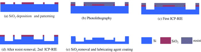
Figure 2 Fabrication process of two-step Si mold.
Finally a lubricating agent for easier de-molding was applied to the Si mold before performing the embossing process. Figures 3 and 4 show the scanning electron microscope (SEM) images of Si mold structures.

Figure 3 SEM image of the two-step Si mold.

Figure 4 SEM image of closed up the comb finger parts.
2.3. Hot embossing and bonding
The fabricated silicon molds were used for the hot embossing process. Movable microstructures were hot embossed on PMMA material. The entire hot embossing procedure and condition parameters are as below:
- Set up a silicon mold and PMMA sheet of 1 mm into a chamber and evacuate to a pressure under 40 Torr. This is an important condition to obtain sharp edges of PMMA structure.
- Heat the silicon mold and PMMA at the same time to a temperature of 180 °C and maintain this temperature for 15 min.
- Insert the mold into PMMA and increase the molding force to 2500 N with the molding rate of 0.1 mm min −1. Maintain the molding force of 2500 N for 15 min.
- Cool the mold and PMMA to 80 °C.
- De-molding rate is 0.01 mm min −1 at 80 °C.
- Vent chamber, remove silicon mold and hot embossed PMMA sheet.
Fine structures (down to 2 μm) were successfully embossed, as shown in figure 5. Figure 6 shows the PMMA movable microstructure fabricated by hot embossing using two-steps mold. The silicon mold was not broken after de-molding, and could be re-used for the next hot embossing experiments. The whole processing cycle was about 45 min.
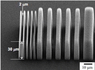
Figure 5 Fine structures were successfully fabricated by the embossing process.
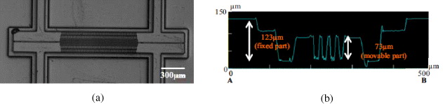
Figure 6 (a) Laser microscope image and (b) cross sectional topography of the embossed PMMA micro structure.
Step heights or the thickness of Si mold and hot embossed PMMA microstructure were measured by laser scanning microscope. Movable parts of Si mold, such as comb finger and beams, had a thickness of about 73 μm. The thickness of the fixed parts is 123 μm. PMMA hot embossed microstructure had a thickness of about 73 μm. The hot embossed microstructure was approximately transferred completely.
After hot embossing, the top surface of PMMA structure was bonded to a PMMA plate by the surface activation method (figure 1(c)) [9]. The surface activation method was performed by treatment of bonding surfaces under vacuum ultraviolet (VUV)/ozone for 10 min. After VUV/ozone treatment, direct bonding was carried out at a temperature of 70 °C and a contact pressure of 4.4 MPa for 10 min. Since the process temperature was low, the deformation of the PMMA microstructures could be prevented.
2.4. Releasing and metallization
After the hot embossed PMMA movable microstructure was bonded to a PMMA substrate, the next step was to release the movable parts of the device, i.e. the remaining PMMA film must be removed. To protect the fragile structures during removing, a reinforcement agent was filled into the structure (figure 1(d)). Next, the remaining PMMA is removed by the polishing method. This method can process a large number of devices at the same time and provides a mirror-finished surface. The polishing process started with 1.0 CR type abrasive (i.e. grit size is 1 μm) and ended up with 0.05 CR type abrasive (grit size is 0.05 μm). Finally, the reinforcing agent was removed in vacuum. Floating PMMA microstructures were released. After the structures were fully released, a thin Au layer was deposited by sputtering to create an electrode for the electrostatic actuator.
A PMMA comb-drive electrostatic microactuator with 200 comb fingers is shown in figure 7 as an example of polymer MEMS fabricated by the hot embossing process.
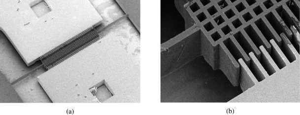
Figure 7 (a) SEM image of PMMA comb-drive electrostatic microactuator with 200 comb fingers. (b) Close up of the comb finger with dimensions of 50×5×60 μm 3.
3. Demonstration of polymer MEMS fabricated by embossing process
3.1. Comb drive electrostatic microactuator
The PMMA comb-drive electrostatic microactuator with 200 comb fingers fabricated by the hot embossing process (figure 1) is shown in figure 7. The comb drive microactuator was placed under a microscope with a digital camera. A high-voltage generator was connected to the movable parts and fixed parts of the actuator. A probe electrode was located close to the suspension beam of the movable parts. The initial gap between the fingers was 5 μm. Driving test results are shown in figure 8. Large displacement was obtained for each applied voltage as compared to the theoretically predicted displacement for a silicon device, which has the same dimensions as the PMMA device. Test results showed that the actuator operated well without sticking, and a displacement of 11 μm at a drive voltage of 100 V was obtained. This displacement is 20 times larger than that of an identical silicon device.
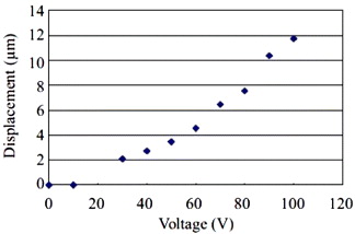
Figure 8 Driving test results of a PMMA comb-drive electrostatic micro actuator.
3.2. Torsional micro mirror device
A PMMA torsional micro mirror device, which consists of a mirror plate driven by vertical comb actuators, was fabricated by the hot embossing process. Figure 9 shows the structure of a torsional micromirror device. The mirror plate is suspended by two torsion bars. The mirror plate can rotate reciprocally around the torsion bars by electrostatic force generated by the vertical comb-drive actuators located at both sides of the mirror plate. The vertical comb actuators are formed by pushing down the fixed comb fingers to create a vertical distance offset between the fixed and movable comb fingers. Dimensions of a finger are 60×5× 60 μm 3 (L×W×T), the gap and overlap between two fingers are 5 μm and 50 μm, respectively, and dimensions of torsion bar are 200×10×60 μm 3. The size of the mirror plate is 1×1 mm 2. The gap between movable structure layer and the substrate is about 30 μm (figure 10).
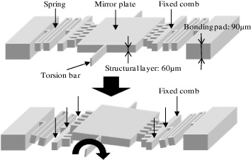
Figure 9 Structure of a torsional micromirror device.
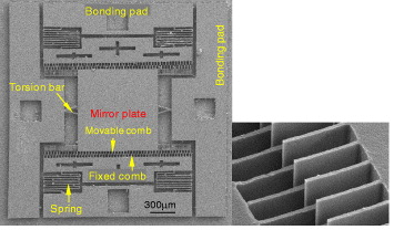
Figure 10 SEM images of PMMA torsion mirror (left), and vertical comb actuator (right) with vertical offset is 25 μm.
The relation between the applied voltage and the mirror rotational angle was a quadratic function with parabolic curve as shown in figure 11. Maximum angle was 3.5° obtained at a driving voltage of 67 V. With higher applied voltage, the rotation angle was unchanged. This means that the edge of the mirror had touched the substrate. If voltage is applied to the actuator at the other side, the total angle is 7°.
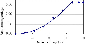
Figure 11 Relation between the applied voltage and the mirror rotation angle. Resonant frequency was calculated to be 3.5 kHz.
3.3. Chevron-shaped thermal microactuator
A PMMA chevron-shaped thermal microactuator was fabricated. Figure 12 shows a schematic of the thermal microactuator. The thicknesses of movable parts were 50 μm. The movable shuttle was supported and thermally actuated by eight beams in a chevron-shaped structure with an initial angle of 1° [10]. Beam length was 2000 μm and beam width was 25 μm. When electric current flowed to the beams, the PMMA beams were thermally expanded due to resistive heating of a thin gold layer deposited surround the beams; as a result, the central shuttle is displaced. Figure 13 shows a chevron-shaped thermal microactuator fabricated by the hot embossing process.
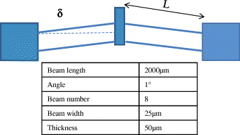
Figure 12 Schematic of chevron-shaped thermal microactuator.
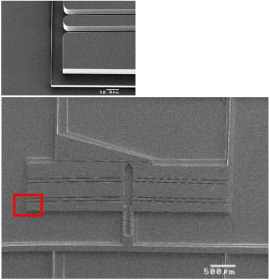
Figure 13 Image of Si mold for chevron-shaped thermal microactuator fabricated by the hot embossing process.
The operational test result is shown in figure 14. The displacement of the shuttle was 10.5 μm for a power consumption of 30 mW. The displacement was about five times larger than that of the Si counterpart [11] at the same power consumption. The displacement is smaller than might be expected due to the poor thermal conduction from the gold thin film heater to entire volume of PMMA beam.
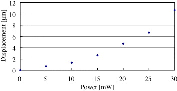
Figure 14 Operational test result of chevron-shaped thermal microactuator.
3.4. Polymer microaccelerometer
A polymer microaccelerometer can also be fabricated by the embossing process. Figure 15 is an SEM image of the PMMA microaccelerometer structure after the hot embossing process. The microaccelerometer consists of a mass suspended by four beams. The mass can move laterally upon an application of acceleration, therefore, the gaps of comb electrodes are changed, leading to the change of capacitance. Capacitance change is then converted to output voltage through a C-V converter circuit. Dimensions of an electrode finger are 110×5×60 μm 3 (L×W×T), gap between the two fingers is 5 μm and 15 μm, and the dimensions of the folded-beams are 1040×10×60 μm 3 (L×W×T). The size of the mass is 1.5×1.5 mm 2. The gap between device layer and the substrate is about 50 μm.
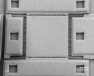
Figure 15 SEM image of PMMA microaccelerometer structure after the hot embossing process.
The PMMA microaccelerometer was preliminarily characterized by rotating it from 0° to 90° and the capacitance change was measured. The output is shown in figure 16. Capacitance changes of 10% (or 0.4 pF) were obtained when accelerations of 1G were applied (figure 16).
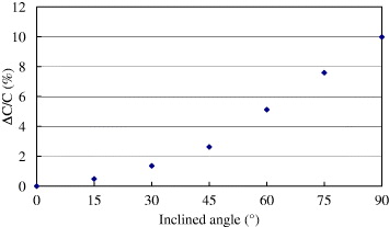
Figure 16 Capacitance changes of 10% (or 0.4 pF) at accelerations of 1G.
4. Conclusions
This research is the early stage of the initiation of R&D on polymer MEMS. Polymer materials have several advantages over silicon, such as lower material costs, transparency, biocompatibility, and biodegradability, etc. Also, soft and high thermal expansion properties are useful for actuators, since it requires less power to create the same displacement compared to their silicon counterparts, and therefore, this can save energy. A PMMA is utilized for polymer MEMS material as the first stage. The next stage will be shifted to the bio-base material originated plant from petrochemicals.
A polymer MEMS process has been developed using hot embossing and precision machining. A two-step silicon mold was fabricated by bulk micromachining. MEMS structures were formed on a PMMA plate by hot embossing. MEMS structures less than 2 μm were successfully embossed. The PMMA layer that remained after hot embossing was removed by a polishing process to release the movable parts. The device structures were coated with a gold layer for the electrode.
Various MEMS devices such as comb-drive electrostatic microactuator, torsional micromirror device, chevron-shaped thermal microactuator and polymer microaccelerometer were fabricated to demonstrate excellent potential of polymer. A PMMA movable microstructure has been successfully fabricated on PMMA by the hot embossing and polishing process. Several advantages of this technique in our experiments can be summarized as follows: (i) the whole process is simple and low cost; (ii) reproduction is easy; (iii) the PMMA structure has higher flexibility compared with the counterpart made of silicon; (iv) the driving voltage is also much lower compared with silicon-based devices because PMMA has a lower Young's modulus; (v) the device surface is very smooth.
Because this work is still at an early stage of our research, there are several problems that need to be solved to improve the performance of polymer-based microaccelerometers, such as reliability and repeatability.
It is necessary to develop the foundation of a sustainable production system in the global scale for the future of human life. Nowadays, in semiconductor and advanced technology based industries, silicon and petroleum-based polymers are being used as key materials, but unfortunately, these materials are not sustainable and not environmentally friendly. Considering the above facts, it is necessary to initiate research on MEMS with environmentally friendly micro-nano machining technology using bio-based polymer materials, and the industrialized technology of applied devices into a wide range of human society in the near future.