
Abstract
A silicon nanowire field-effect transistor based sensor (SiNW-FET) has been proved to be the most sensitive and powerful device for bio-detection applications. In this paper, SiNWs were first fabricated by using our recently developed deposition and etching under angle technique (DEA), then used to build up the complete SiNW device based biosensor. The fabricated SiNW biosensor was used to detect DNA of genetically modified maize. As the DNA of the genetically modified maize has particular DNA sequences of 35S promoter, we therefore designed 21 mer DNA oligonucleotides, which are used as a receptor to capture the transferred DNA of maize. In our work, the SiNW biosensor could detect DNA of genetically modified maize with concentrations down to about 200 pM.
Export citation and abstract BibTeX RIS

Content from this work may be used under the terms of the Creative Commons Attribution-NonCommercial-ShareAlike 3.0 licence. Any further distribution of this work must maintain attribution to the author(s) and the title of the work, journal citation and DOI.
1. Introduction
Over several years, there has been a steady increase in reports of functional nanoscale (∼10–100 nm) materials, such as carbon-nanotubes (CNTs) [1, 2] and silicon-nanowires (Si-NWs) [3, 4]. One- and two-dimensional structures, such as CNT devices and NW devices, are technologically compelling due to their reported highly sensitive label-free detection of biomolecules in aqueous phase [5–12] and suitability for large-scale high-density integrated electronics [4]. Silicon nanowire devices are advantageous to CNT devices because there is a well-established knowledge base about silicon, and silicon-related materials, such as silicon dioxide and silicon nitride, well-characterized surfaces and interfaces, and mature planar microfabrication technologies.
The refinement and development of new microfabrication techniques, combined with the development of new nanofabrication techniques, are fueling the rapid development of nanoscale materials, such as Si-NWs, with unprecedented precision and repeatability. There are two broad classifications for NW fabrication: bottom-up and top-down. The bottom-up approach attempts to assemble the necessary device elements at the atomic level. A large number of materials, such as common semiconductor materials like Si, Ge, and ZnO, and many others, have been successfully synthesized into nanostructures over the last decade [13, 14]. A key bottom-up process constraint in the synthesis of nanostructures is crystallization, which involves nucleation and growth as the basic steps. The vapor–liquid–solid growth method is commonly used to generate single crystal nanostructures in large quantities [15]. Gas mixtures containing dopants, such as boron and phosphorus, have also be introduced to the precursor gas mixture, resulting in in-situ doped p-type or n-type Si-NWs, respectively [16]. The main disadvantages of bottom-up manufactured NWs include the lack of controlled growth into high-density arrays, which typically requires transfer and assembly of devices on separate substrates, and challenges in reproducibly forming high quality electrical contacts.
Top-down fabrication technology, the standard technique for semiconductor manufacture, has been used to realize NWs from Si [7–9, 11, 12], Au and Ag [17], as well as many others. Top-down fabrication is based on micromachining processes consisting of deposition, etching and ion-beam milling on planar substrates. Patterning is typically done using UV- and DUV-photolithography and commonly combined with advanced nanolithography techniques, such as electron beam lithography (EBL) or focused-ion-beam (FIB) to realize feature sizes down to 10 nm [18] and ultimately down to a few nm [19]. Although EBL and FIB techniques are valuable methods for a research environment, they are, in general, not amenable to large-scale manufacturing. Replication top-down fabrication techniques, such as nanoimprint lithography [20], are capable of combining the resolution of EBL with large area pattern formation. High-density Si-NW arrays have been reported with 15 nm wide Si nanowires at a 34 nm pitch using the SNAP pattern transfer technique [21]. Nanoimprint lithography, being a promising technique, still requires significant development for general application to nanopatterning. Impurity doping of the top-down fabricated Si-NWs can be achieved through the well-established ion-implantation or using spin-on-dopant-containing thin films [4].
Although there has been significant progress in realizing functional Si-NWs, using both bottom-up and top-down approaches, the manufacturing methods can be significantly simplified using a combination of conventional micromachining and new nanofabrication techniques. In this paper, we present a new wafer-scale nanofabrication technology, deposition and etching under angles, DEA, capable of realizing Si-NWs with lateral dimensions down to 100 nm and lengths up to 1 mm [22–26]. The DEA technology, which uses standard micromachining processes, requires a single conventional contact-mode photolithography step (an additional lithography step is required to make the electrical contacts). Functional Si-NWs have been realized with the DEA technology resulting in moderately dense device arrays (spacing down to ∼500 nm), tunable nanowire conductance and low contact resistance. Finally, we present our result of the detection of genetically modified maize DNA by using the fabricated SiNW devices. The DNA with concentrations down to about 200 pM has been detected.
2. Fabrication of Si-NW
One of the key advantages of top-down Si-NW fabrication is that large (>1 μm 2) contacting regions can be created easily, which is important for reliable high quality electrical contacts [22–27]. The key process steps of the DEA top-down Si-NW fabrication process [22–26] are shown schematically in figure 1. This requires two conventional contact-mode photolithography steps to form the Si-NW devices. Another advantage of the top-down Si-NW fabrication is the commercial availability of high quality silicon-on-insulator (SOI) substrates, which are available from many different vendors. The Si-NWs presented in this article are manufactured from SOI wafers (SOITEC) with a 70 nm thick device layer Si(100) and 140 nm buried oxide (BOX) layer. The first step of the process is to reduce the thickness of the device layer silicon to 40 nm using a thermal oxidation-wet etching thinning process. The remaining silicon device layer is then doped by ion implantation (energy: 35 kV, ion: BF 2 +, dose: 1014 cm -2, angle: 7°) and subsequently annealed to form the uniform p-type silicon layer (950 °C, 100% N 2) with a target doping concentration of ∼5×1018 cm -3, which is sufficient to form an ohmic electrical contact at the metal-silicon interface [27]. A 20 nm thick thermal oxide (SiO 2) is reactively grown with wet-oxidation (950 °C) on the silicon device layer. Next, a 20 nm layer of stoichiometric silicon nitride (Si 3 N 4) is deposited in a low-pressure chemical vapor deposition (LPCVD: 200 mTorr, 800 °C, 22 sccm SiH 2 Cl 2, 66 sccm NH 3) reactor directly on the SiO 2 surface (figure 1).

Figure 1 Single-mask silicon nanowire DEA fabrication process diagram.
A photolithographically (EVG 620, Electronic Visions Group) defined window, l w ∼3 μm, is etched (20 mTorr, 150 W, 20 sccm CHF 3, 5 sccm O 2) using reactive ion etching (RIE) in the Si 3 N 4 layer, as shown in figure 1(b). The width W w can be scaled down to sub-micron dimensions with refined lithography conditions. The exposed SiO 2 layer is wet etched in dilute hydrofluoric acid (5%) to form the undercut region between the Si 3 N 4 and silicon layers (figure 1(c)). A thin metal (Cr) layer is then electron-beam evaporated at a 45° angle with respect to the substrate (figure 1(d)). Ion beam milling (Ar, 10 kV) is subsequently done at −45° to remove a portion of the metal layer in the cavity, which results in a hard-etch metal mask layer (figures 1(e) and 1(f)). The remaining Si 3 N 4 and SiO 2 layers are removed using a combination of RIE and wet etching, shown in figures 1(f) and (g). Figure 2(a) shows a scanning electron micrograph (SEM) of a ∼33 nm wide metal hard mask.

Figure 2 (a) SEM image of metal hard mask prior to etching the silicon device layer with lateral width ∼33 nm. (b) SEM image of a bare silicon nanowire with width of about 40 nm. The fabricated nanowire has metal contact pads at both ends for further connection to the outer electronic control.
A second lithography step is then used to mask contact regions at the ends of the Si-NW. The Si-NW structures are finally formed using RIE (100 mTorr, 200 W, 20 sccm SF 6, 5 sccm O 2). The metal hard mask layer is removed in a wet etchant (CR-14, Transene Co., Inc.). The Si-NW is shown in figure 2(b). The exposed silicon surfaces have been oxidized to form a thin (∼5 nm) SiO 2 electrical isolation layer using conventional dry oxidation (950 °C, 5 min.). The oxide isolation layer is removed at the electrical contact regions in a dilute hydrofluoric acid etch (5%) and a Ni/Pt (20 nm/180 nm) layer is deposited and subsequently annealed (450 °C, 20 min) to form a NiSi silicide at the Ni-Si interface.
Functional Si-NW devices with widths down to ∼40 nm have been realized and we are working to reduce the lateral dimensions to about 10 nm with refinements to the etching and milling processes. Finally, a thin (∼2 μm) polyimide layer was spin coated and patterned to electrically isolate the metal contact regions from the electrolyte samples for DNA measurement.
2.1. Electrical characterization of the fabricated Si-NW device
The electrical characteristics of the fabricated Si-NW devices have been measured to quantify the following: (i) doping concentration and resistivity of the silicon body layer, (ii) electrical contact behavior with a 2-contact device, and (iii) contact resistance evaluations using a modified transfer-length-method (TLM) [27–30]. Electrical measurements were performed using dc and low frequency signal sources. The resistance measurements were performed on a probe station (SUSS EP6) and the i–ν characteristics were measured with a semiconductor parameter analyzer (HP/Agilent 4155C).
The resistivity of the Si-NW body layer is used to evaluate R s after all thermal processing steps, which can lead to lower doping levels, especially in the case of boron doped silicon with a segregation coefficient of less than unity, which means that the boron can easily segregate out of the silicon into the surrounding SiO 2 layers at elevated temperatures. A conventional 4-point probe structure was used to measure the resistivity ρ s , which is used to eliminate the effect of R c in the measurement. For 50 μm long Si-NWs, the average measured resistivity is ρ s =2.84±0.58×10⁻² Ωcm (10 samples), which is translated into N a ≈ 2×1018 cm -3, with A c =8.0×10⁻¹⁵ m 2 (two parallel Si-NWs 3 ) estimated from SEM imaging. It should be noted that the target doping level was 5×1018 cm -3, which demonstrates the importance of careful device design, fabrication and characterization.
The electrical behavior of the metal-silicon contacts is evaluated by measuring the bipolar i–ν characteristics. Figure 3 shows examples of the measured i–ν curves from Si-NW devices, with varying lengths, demonstrating the linear Ohmic behavior of the electrical contacts for dc and low frequency sources. Ohmic contacts to silicon are characterized by linearity and low voltage drops, which are achieved when the device impedance is dominated by the silicon body layer and not the metal–silicon interface [27]. The slope of the i–ν measurements corresponds to the total Si-NW resistance R T ≈Δv d /Δi d , which contains resistance from the Si-NW device and contributions due to the metal-semiconductor contacts. The measured devices show the linear i–ν characteristics and symmetric zero-crossing behavior. Meanwhile, the contact resistance was estimated with a modified TLM where separate Si-NWs with varying lengths (L1, L2 and L3) are used. The measured data show a relatively large contact resistance R c =20±9 kΩ (average specific contact resistivity ρ c =3.1×10⁻² Ωcm 2) with large variation in contact resistance from device to device. The measured average specific contact resistance can be reduced substantially with further refinement to the fabrication process [28].
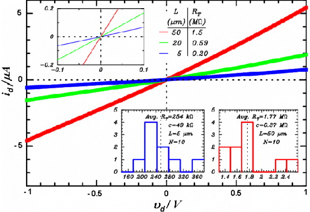
Figure 3 Measured i–ν curves (2-probe measurement) of Si-NW devices with varying lengths. The upper inset shows the zero-crossing point of the measured i–ν data. The lower insets show measured total resistance histograms for Si-NWs with lengths L=5 μm and 50 μm.
The slope of the R T -L data has also been used to estimate the Si-NW device resistivity (some devices exhibited a slightly different slope) ρ s =2.86±0.36×10⁻² Ωcm (8 samples), which is consistent with the 4-point measurements. Clearly, further refinements are required to reduce the contact resistance and device variability. For a Si-NW with length L=50 μm, the contact resistance represents about 2% of the total Si-NW resistance. From the measured resistivity, with the 4-point contact structures, and the measured cross-sectional area A c , we find that there is wide variation of R T from device to device, which requires further investigation.
The formation of good electrical contacts to silicon using planar fabrication technology requires consideration of the metal-silicon potential barrier, due to the work function difference, and surface contamination. A practical solution to reduce the height of the metal-silicon potential barrier is to properly choose a metal layer with a low work function difference. The width of the potential barrier can be substantially reduced by doping the surface with impurity concentrations more than 5×1018 cm -3, for p-type silicon, and more than 1019 cm -3, for n-type silicon, such that the carrier transport across the metal-semiconductor interface is dominated by quantum-mechanical tunneling and the width of the barrier is narrow. Surface contamination is an important issue and can be minimized with proper cleaning procedures as well as creating large contacting surface areas, such that some degree of contamination is tolerable without reducing the device performance.
3. Detection of genetically modified maize DNA by using Si-NW devices
3.1. Surface modification for Si-NW devices
Although the NW FETs described above will be sensitive to the surrounding environment, they will not have the desired molecular recognition properties. The surface of the sensing element (NW) thus needs to be modified so that the device acquires specific recognition toward a desired analyte [31]. The method used to functionalize the SiNWs without an oxide coating is illustrated in figure 4. Actually, a procedure reported previously was used to functionalize hydrogen-passivated SiNWs with tert-butyl allylcarbamate [32]. Hydrogen-terminated SiNWs were prepared by etching away the SiO 2 coating by exposing the SiNW device to 1% HF for 3 min. The H-terminated SiNWs were immediately covered with a thin film of the tert-butyloxycarbonyl (t-BOC) protected amine and quickly transferred to a N 2-purged Teflon reaction cell where they were illuminated with UV light (254 nm) for 3 h. The SiNW device was then rinsed in chloroform for 15 min at 50 °C and then twice in methanol at room temperature, each time for 5 min. The deprotection of t-BOC protected amine could be carried out by immersing the SiNW device in 10% trifluoroacetic acid (TFA) in methylene chloride for 2 h, subsequently treating the SiNW device with 1% aqueous ammonium hydroxide for 5 min followed by a rinse in pure H 2 O.

Figure 4 Illustration of DNA immobilization and DNA–DNA hybridization on the SiNW surface.
3.2. Immobilization of DNA receptor
The main goal of our study was the detection of DNA of genetically modified maize. Therefore, we used DNA that NH2-modified at 5' position as a receptor. This receptor has a sequence of 5'-NH 2-C 6-CCACGTCTTCAAAGCAAGTGG-3'. The DNA complementary for this receptor therefore was 5' CCACTTGCTTTGAAGACGTGG 3'.
To covalently immobilize the receptor on the SiNWs, a bifunctional linker of glutaraldehyde was employed to bind its one end to the SiNW amines, and leave the other end to bind the amine-terminated DNA receptor [31–33]. The SiNW device was treated with 2% glutaraldehyde in H 2 O for 1 h, and rinsed with pure H 2 O. The SiNW device was then incubated in the receptor solution of 10 μm in an ambient condition at room temperature overnight. The Si-NW contained chips were washed three times with 1×SSC, 5 min each after immobilization of the receptor. Unreacted aldehyde surface groups were subsequently passivated by reaction with ethanolamine, in the presence of 4 mM cyanoborohydride for 2 h, and rinsed with 1×SSC. After this step, the freshly prepared chips were used immediately for the DNA hybridization measurements.
3.3. Electrical measurement of the DNA hybridization
Electrical measurements for the sensing experiments were carried out in a DNA complement solution with concentration 100–1000 pM in 0.05×SSC by recording the current flow through the SiNW devices. As the used SiNW is p-type, the hybridization of negatively charged DNA will thus increase the observed current [22, 31–33]. The I–t characteristics through the SiNW devices were measured with a HP/Agilent (4155C) connected to a probe station (SUSS, EP6). During the measurements, the SiNW device was biased with a voltage of -20 V. Figure 5 shows that the hybridization occurred between the DNA receptor and DNA complementary, indicated by the increase in the observed current. As can be seen, the current increased about 4 nA (from 80 to 84 nA) after the chip was exposed to DNA complement solution for about 280 s. The hybridization processes took place for about 5 min before the current became stable. This observation of the current changing really proves that there was capture between the receptor and complementary DNAs.

Figure 5 Measured I–t curve shows DNA–DNA hybridization with 1000 pM complementary DNA. The upper line shows the case where no DNA–DNA hybridization was taken place.
4. Conclusion
A silicon nanowire field-effect transistor based sensor (SiNW-FET) was successfully fabricated by using the deposition and etching under angle technique (DEA). The fabricated devices showed good electrical characteristics for semiconductor nanowires with a good ohmic contact. The fabricated SiNW was then used to build up the complete SiNW device based biosensor for the detection of DNA of genetically modified maize. The measurements show that the SiNW biosensor could detect DNA of genetically modified maize with concentrations down to about 200 pM. Recently, the work has been ongoing in our laboratory to improve the device sensitivity for the ultrasensitive detection of other biological species, like biomarkers for diagnosing of several diseases.
Acknowledgment
The authors thank KC.04.12/06–10 for financial support.
Footnotes
It should be noted that many of the tested devices had two Si-NWs per electrical contact.